Integrated circuit with improved static noise margin

Active Publication Date: 2009-12-22
XILINX INC
View PDF3 Cites 17 Cited by
  • Summary
  • Abstract
  • Description
  • Claims
  • Application Information

AI Technical Summary

Problems solved by technology

CMOS technology has been shrinking, that is, the devices and the separation between devices has been getting smaller.
However, this is contrary to the desired advantages (e.g., higher cell density per silicon area) b

Method used


Image

  • Integrated circuit with improved static noise margin
  • Integrated circuit with improved static noise margin
  • Integrated circuit with improved static noise margin

Examples


Embodiment Construction
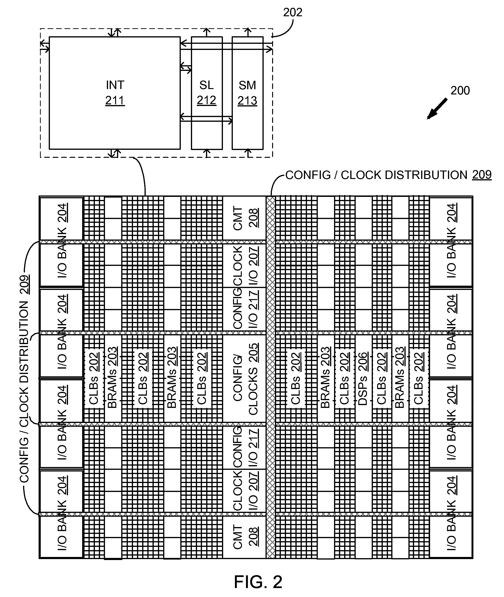
An Exemplary FPGA

[0023]FIG. 2 illustrates an FPGA architecture 200 implementing one or more embodiments of the invention. The FPGA architecture 200 includes a large number of different programmable tiles including multi-gigabit transceivers (not shown), configurable logic blocks (CLBs 202), random access memory blocks (BRAMs 203), input / output blocks (IOBs) organized into I / O banks 204, configuration and clocking logic (CONFIG / CLOCKS 205), digital signal processing blocks (DSPs 206), specialized input / output blocks (I / O 217 and 207) (e.g., configuration ports and clock ports), and other programmable logic 208 such as digital clock managers, analog-to-digital converters, system monitoring logic, and so forth. Some FPGAs also include dedicated processor blocks (not shown).

[0024]In some FPGAs, each programmable tile includes a programmable interconnect element (INT 211) having standardized connections to and from a corresponding interconnect element in each adjacent tile. Therefore, th...


PUM


Abstract

A static random access memory (“SRAM”) has a plurality of SRAM cells connected to a word line. A static noise margin (“SNM”) detector controls a pull-down transistor that selectively couples the word line to a ground path. The SNM detector is configured to produce a first output signal in response to a SNM event that couples the word line to the ground path, and otherwise produces a second output signal that de-couples the word line from the ground path.

Description

FIELD OF THE INVENTION[0001]This invention relates generally to static random access memory (“SRAM”), and more specifically to operating an SRAM array to avoid errors caused by static noise margin (“SNM”).BACKGROUND OF THE INVENTION[0002]CMOS circuits are used in a variety of integrated circuit (IC) applications. A CMOS process can be used to fabricate many different sorts of functionality, such as memory, logic, and switching, and thus CMOS techniques are particularly desirable in applications where an IC includes several different types of functional blocks.[0003]One family of ICs employing CMOS fabrication techniques are programmable logic devices (PLDs). PLDs are a well-known type of integrated circuit that can be programmed to perform specified logic functions. One type of PLD, the field programmable gate array (FPGA), typically includes an array of programmable tiles. These programmable tiles can include, for example, input / output blocks (IOBs), configurable logic blocks (CLBs...

Claims


Application Information

Patent Timeline
IPC IPC(8): G11C7/02
CPCG11C7/02H03K19/17764H03K19/1776G11C11/413
Inventor PENG, TAO
Owner XILINX INC
Why Eureka
Try Eureka