Drive circuit for reducing inductive kickback voltage

a technology of inductive kickback voltage and drive circuit, which is applied in the direction of pulse generator, dc motor rotation control, pulse technique, etc., can solve the problems of unfavorable zener diodes, damage to components, and inability to integrate zener diodes in chips, etc., to achieve the effect of reducing chip size and quick reducing kickback voltag

Inactive Publication Date: 2009-12-29
EUTECH MICROELECTRONICS
View PDF11 Cites 55 Cited by
  • Summary
  • Abstract
  • Description
  • Claims
  • Application Information

AI Technical Summary

Benefits of technology

[0019]It is therefore one object of the invention to provide a drive circuit comprising two comparators which are adapted to sense kickback voltage generated in an inductive load and conduct two field-effect transistors connected to ground in a very short period of time so as to quickly reduce the kickback voltage to a minimum value. The invention can also reduce chip size.
[0020]It is another object of the invention to provide a drive circuit comprising a comparator which is adapted to sense kickback voltage generated in an inductive load and conduct two field-effect transistors connected to ground in a very short period of time so as to quickly reduce the kickback voltage to a minimum value. The invention can also reduce chip size.

Problems solved by technology

The kickback voltage can apply to the drive system (i.e., circuit) to undesirably increase power consumption.
However, the kickback voltage may exceed the maximum voltage allowed by other components of the circuit 5, resulting in a damage to these components.
However, it is not always possible of integrating a Zener diode in a chip because many semiconductor manufacturing processes do not support such technology.
This can result in an increase in the chip manufacturing cost.
Otherwise, a quiescent current of a circuit may be adversely affected.
Also, the addition of a Zener diode has the drawbacks of greatly increasing the chip manufacturing cost.

Method used


Image

  • Drive circuit for reducing inductive kickback voltage
  • Drive circuit for reducing inductive kickback voltage
  • Drive circuit for reducing inductive kickback voltage

Examples


Embodiment Construction

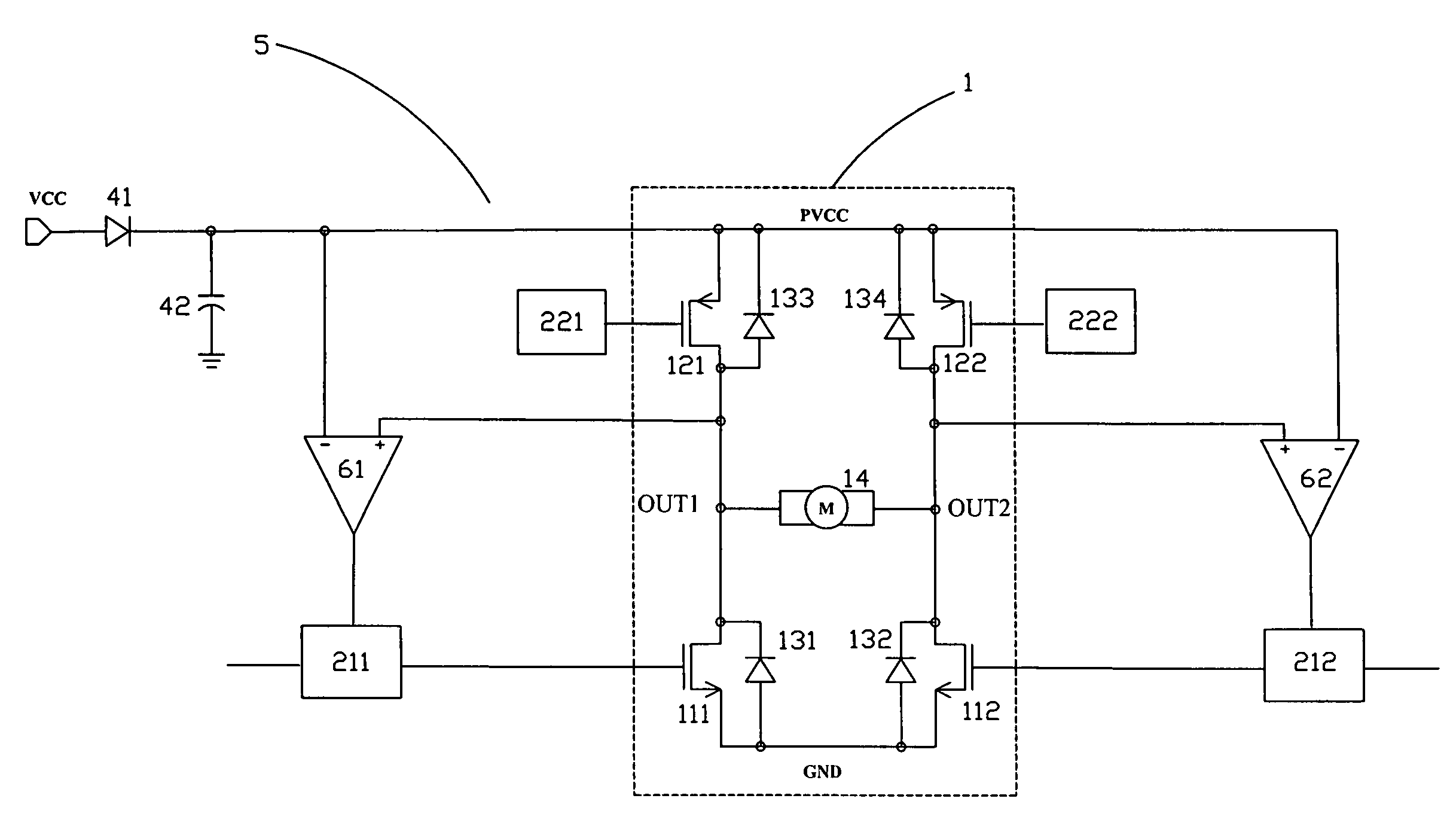
[0035]Referring to FIGS. 5 and 6, a drive circuit for reducing kickback voltage generated in an inductive load in accordance with a first preferred embodiment of the invention is shown. The drive circuit 5 comprises an H-shaped transistor assembly 1, first and second comparators 61, 62; and first, second, third, and fourth logic controls 211, 212, 221, 222. The first comparator 61 comprises a positive input 61P1, a negative input 61P2, and an output 61P3. The second comparator 62 comprises a positive input 62P1, a negative input 62P2, and an output 62P3. The first logic control 211 comprises first and second inputs 211P1, 211P2 and an output 211P3. The second logic control 212 comprises first and second inputs 212P1, 212P2 and an output 212P3. The third logic control 221 comprises an input 221P1 and an output 221P2. The fourth logic control 222 comprises an input 222P1 and an output 222P2.

[0036]The H-shaped transistor assembly 1 comprises first, second, third, and fourth inputs 11P1...


PUM


Abstract

In one embodiment a drive circuit includes two comparators which are adapted to sense kickback voltage generated in an inductive load and conduct two field-effect transistors connected to ground in a very short period of time so as to quickly reduce the kickback voltage to a minimum value. In another embodiment only one comparator is provided.

Description

BACKGROUND OF THE INVENTION[0001]1. Field of Invention[0002]The invention relates to kickback voltage reduction circuits and more particularly to a drive circuit incorporating one or two comparators adapted to sense kickback voltage generated in an inductive load and conduct two field-effect transistors connected to ground in a very short period of time so as to quickly reduce the kickback voltage.[0003]2. Description of Related Art[0004]Many inductive load drive systems for disk drive, fan motor drive or the like employ a drive circuit for reducing kickback voltage generated therein. A kickback voltage is generated when a current flowing through an inductive load is suddenly changed. The kickback voltage can apply to the drive system (i.e., circuit) to undesirably increase power consumption.[0005]FIG. 1 shows a conventional drive circuit 5 for reducing kickback voltage generated in an inductive load. The circuit 5 comprises an H-shaped transistor assembly 1 including transistors (e...

Claims


Application Information

Patent Timeline
Patent Type & Authority Patents(United States)
IPC IPC(8): H03K17/56
CPCH02P7/0044H03K17/6874H03K17/08142H02P7/04
Inventor HSIAO, KOSUN, CHIANG
Owner EUTECH MICROELECTRONICS
Why Eureka
Try Eureka