CMOS image sensor and method for manufacturing the same

a technology of image sensor and manufacturing method, which is applied in the field of cmos (complementary metal oxide silicon) image sensor, can solve the problems of high power consumption, complicated drive mode, and complicated manufacturing process of ccd, and achieve the effects of reducing or preventing damage to the photodiode, and enabling the scaling down of the pixel

Inactive Publication Date: 2010-01-26
DONGBU ELECTRONICS CO LTD
View PDF7 Cites 7 Cited by
  • Summary
  • Abstract
  • Description
  • Claims
  • Application Information

AI Technical Summary

Benefits of technology

[0036]The present invention has been made to solve the above problems occurring in the related art, and therefore, it is an object of the present invention to provide a CMOS image sensor and a method for manufacturing the same, capable of reducing or preventing damage to the photodiode and improving a pixel design margin to enable scale down of the pixel.

Problems solved by technology

However, CCDs may have has various disadvantages, such as a complicated drive mode, high power consumption, and so forth.
Also, the CDD is generally manufactured using multi-step photo processes, so the manufacturing process for the CCD can be complicated.
In addition, since it can be difficult to integrate certain circuits, such as a controller, a signal processor, and an analog / digital converter (AID converter) onto a single chip of the CCD, the CCD may not be advantageous for compact-size products.
However, the above connection method may cause damage to the photodiode when forming the contact hole in the photodiode area.
In addition, since the photodiode area is connected to the gate electrode by means of the metal interconnection through four ohmic contacts, it can be challenging to improve the pixel design margin.

Method used


Image

  • CMOS image sensor and method for manufacturing the same
  • CMOS image sensor and method for manufacturing the same
  • CMOS image sensor and method for manufacturing the same

Examples


Embodiment Construction

[0044]Hereinafter, a CMOS sensor and a manufacturing method thereof according to the present invention will be described in detail with reference to the following drawings.

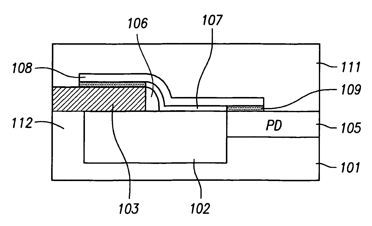
[0045]FIG. 4 is a sectional view taken along line IV-IV′ of FIG. 2 to show the CMOS image sensor according to the present invention.

[0046]As shown in FIG. 4, the CMOS image sensor includes an isolation layer 102 formed in an isolation area of a p-type semiconductor substrate 101 having an active area 112 and the isolation area, a source follower transistor having a gate electrode 103 extending across a part of the isolation layer 102 and the active area 112, a photodiode area (PD) 105 formed in a part of the active area of the semiconductor substrate 101, an insulating sidewall spacer 106 formed at sides of the gate electrode 103, a metal silicide layer 109 formed on the top surface of the gate electrode 103 and a part of a surface of the photodiode area 105 adjacent to the gate electrode 103, a metal layer 107 el...


PUM


Abstract

Disclosed are a CMOS image sensor and a method for manufacturing the same, for reducing or preventing damage to a photodiode and improving a pixel design margin to achieve scale down of a pixel. The CMOS image sensor includes an isolation layer in a semiconductor substrate, a gate electrode crossing a part of the isolation layer and the active area, a photodiode area in the active area, an insulating sidewall spacer on sides of the gate electrode, a metal silicide layer on the gate electrode and at least part of a surface of the photodiode area adjacent to the gate electrode, a metal layer electrically connecting the gate electrode to the photodiode area, and a dielectric layer on the entire surface of semiconductor substrate.

Description

[0001]This application claims the benefit of Korean Application No. 10-2005-0096365, filed on Oct. 13, 2005, which is incorporated by reference herein in its entirety.BACKGROUND OF THE INVENTION[0002]1. Field of the Invention[0003]The present invention relates to a CMOS (complementary metal oxide silicon) image sensor. More specifically, the present invention relates to a CMOS image sensor and a method for manufacturing the same, capable of simplifying the structure of the CMOS image sensor while achieving scale down of a pixel.[0004]2. Description of the Related Art[0005]In general, an image sensor is a semiconductor device for converting optical images into electric signals, and it may be classified as a charge coupled device (CCD) or a CMOS image sensor.[0006]The CCD has a plurality of photodiodes (PDs), which are arranged in the form of a matrix in order to convert optical signals into electric signals. The CCD includes a plurality of vertical charge coupled devices (VCCDs) prov...

Claims


Application Information

Patent Timeline
Patent Type & Authority Patents(United States)
IPC IPC(8): H01L21/8238H01L27/146H04N5/335H04N5/369H04N5/374
CPCH01L27/14609H01L27/14687H01L21/76895H01L27/14636H01L27/14643H01L27/146
Inventor JEON, IN GYUN
Owner DONGBU ELECTRONICS CO LTD
Why Eureka
Try Eureka