Methods for improving uniformity and resistivity of thin tungsten films

a thin tungsten film, uniformity technology, applied in the direction of coatings, basic electric elements, chemical vapor deposition coatings, etc., can solve the problems of limited ability to provide nucleation layers for the deposition of low resistivity tungsten in smaller features with high aspect ratios, and cannot be produced easily and reliably. achieve the effect of low resistivity

Active Publication Date: 2010-02-02
NOVELLUS SYSTEMS
View PDF61 Cites 83 Cited by
  • Summary
  • Abstract
  • Description
  • Claims
  • Application Information

AI Technical Summary

Benefits of technology

[0005]The methods described herein relate to deposition of low resistivity, highly conformal tungsten nucleation layers. These layers serve as a seed layers for the deposition of a tungsten bulk layer. The methods are particularly useful for tungsten plug fill in which tungsten is deposited in high aspect ratio features. The methods involve depositing a nucleation layer by a combined PNL and CVD process. The substrate is first exposed to one or more cycles of sequential pulses of a reducing agent and a tungsten precursor in a PNL process. The nucleation layer is then completed by simultaneous exposure of the substrate to a reducing agent and tungsten precursor in a chemical vapor deposition process. In certain embodiments, the process is performed without the use of a borane as a reducing agent.

Problems solved by technology

The bulk layer is generally deposited more rapidly than the nucleation layer, but cannot be produced easily and reliably without first forming the nucleation layer.
Although CVD and other methods have been able to deposit nucleation layers, their ability to provide nucleation layers for the deposition of low resistivity tungsten in smaller features with high aspect ratios is limited.

Method used


Image

  • Methods for improving uniformity and resistivity of thin tungsten films
  • Methods for improving uniformity and resistivity of thin tungsten films
  • Methods for improving uniformity and resistivity of thin tungsten films

Examples


examples

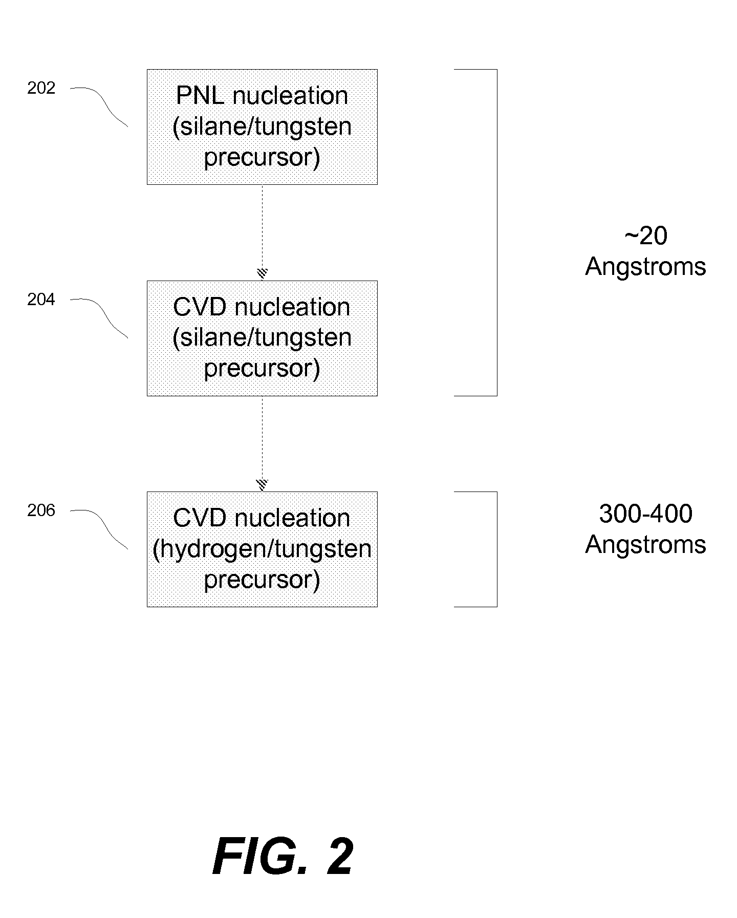
A 350 Angstrom tungsten film was deposited using the sequence given in the following table:

[0031]

LayerProcessPressure, Temp, TimeNucleation2 PNL Cycles40 Torr, 325 C.(SiH4 / WF6)CVD (SiH4 / WF6)40 Torr, 415 C., 2 secondsBulkCVD (H2 / WF6)40 Torr, 415 C., 11 seconds

The resulting film had a non-uniformity of 2.5% and a resistivity of 19 tΩ-cm. This is an improvement over both the CVD-only and PNL-only processes as discussed above.

As indicated above, the PNL portion of the nucleation process does not result in measurable deposition in certain embodiments. This is shown in the below data on the PNL portion:

[0032]

Number of PNLcycles (SiH4 / WF6)TemperatureThickness2325 C.4325 C.14 Angstroms6325 C.36 Angstroms

Although 2 PNL cycles did not result in measurable deposition, it enhances the CVD tungsten nucleation and growth. This is shown in the table below:

[0033]

%Non-uniformityThickness(sheet metalResistivityProcess(Angstroms)resistance)(μΩ-cm)CVD 2s nucleation + CVD37615.0118.9bulkCVD 4s nucleatio...


PUM

PropertyMeasurementUnit
thickaaaaaaaaaa
thickaaaaaaaaaa
pressureaaaaaaaaaa

Abstract

The methods described herein relate to deposition of low resistivity, highly conformal tungsten nucleation layers. These layers serve as a seed layers for the deposition of a tungsten bulk layer. The methods are particularly useful for tungsten plug fill in which tungsten is deposited in high aspect ratio features. The methods involve depositing a nucleation layer by a combined PNL and CVD process. The substrate is first exposed to one or more cycles of sequential pulses of a reducing agent and a tungsten precursor in a PNL process. The nucleation layer is then completed by simultaneous exposure of the substrate to a reducing agent and tungsten precursor in a chemical vapor deposition process. In certain embodiments, the process is performed without the use of a borane as a reducing agent.

Description

FIELD OF INVENTION[0001]This invention relates to methods for preparing tungsten films. The invention is particularly useful for integrated circuit applications that require conformal thin tungsten films having low electrical resistance.BACKGROUND[0002]The deposition of tungsten films using chemical vapor deposition (CVD) techniques is an integral part of many semiconductor fabrication processes. The tungsten films may be used to produce low resistivity electrical connections in the form of horizontal interconnects, vias between adjacent metal layers, and contacts between a first metal layer and the devices on the silicon substrate. In a conventional tungsten deposition process, the wafer is heated to the process temperature in a vacuum chamber, and then a very thin portion of tungsten film, which serves as a seed or nucleation layer, is deposited. Thereafter, the remainder of the tungsten film (the bulk layer) is deposited on the nucleation layer. Conventionally, the bulk layer is ...

Claims


Application Information

Patent Timeline
Patent Type & Authority Patents(United States)
IPC IPC(8): H01L23/48H01L21/44H01L21/4763H01L23/52H01L29/40
CPCC23C16/0281C23C16/08H01L21/28556H01L21/76876H01L23/53266H01L2924/0002
Inventor GAO, JUWENCHAN, LANA HIULUIWONGSENAKHUM, PANYA
Owner NOVELLUS SYSTEMS
Why Eureka
Try Eureka