Reworked integrated circuit device and reworking method thereof

a technology of integrated circuit devices and reworking methods, which is applied in the direction of semiconductor devices, semiconductor/solid-state device details, electrical apparatus, etc., can solve the problems of bridging or breaking circuit connections, yield loss, and complicated fabrication process of integrated circuit devices, so as to efficiently and effectively remove the conductive layer

Active Publication Date: 2010-02-16
UNITED MICROELECTRONICS CORP
View PDF6 Cites 3 Cited by
  • Summary
  • Abstract
  • Description
  • Claims
  • Application Information

AI Technical Summary

Benefits of technology

[0007]It is therefore an objective of the present invention to provide a reworking method to remove defects on integrated circuit devices, thereby reducing costs resulting from wafer scraping.
[0010]Accordingly, the reworking method of the present invention is able to efficiently and effectively remove the conductive layer disposed on the dielectric layer which is to be rebuilt without impairing the reliability of the integrated circuit devices.

Problems solved by technology

The fabrication process of the integrated circuit devices is very complicated.
However, particle contamination occurs during many of the processing steps, and thereby results in yield loss.
These particles can be disposed onto the surface of the respective integrated circuit devices, and resulting in bridging or broken circuit connections between two components, and causing damage to normal functions.
Besides, when the compositions of the deposited film are irregular, the integrated circuit may end up having a rugged surface, with defects such as a hillock or a void formed on the surface.
These defects can result in signal timing discrepancies and undesirable parametric yield loss, thus affecting the quality of the integrated circuit devices thereby failing quality inspection, and is to be assessed as defective products, and thus cannot be transferred to the next production step.
Moreover, sometimes entire batch of wafers having defects must be scraped.
As a result, scraping of wafers not only increases product cost, reduces utilization efficiency of equipments, and delays delivery of the products.

Method used


Image

  • Reworked integrated circuit device and reworking method thereof
  • Reworked integrated circuit device and reworking method thereof
  • Reworked integrated circuit device and reworking method thereof

Examples


Embodiment Construction

[0018]Hereinafter, preferred embodiments of the present invention will be described with reference to the accompanying drawings, in which components with substantially the same functions are identified by the same reference numeral for the sake of simplicity. It should be noted, however, that the present invention is in no way limited to the following illustrative embodiments.

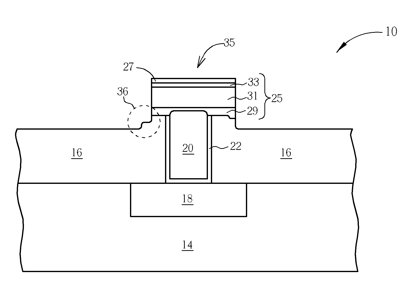
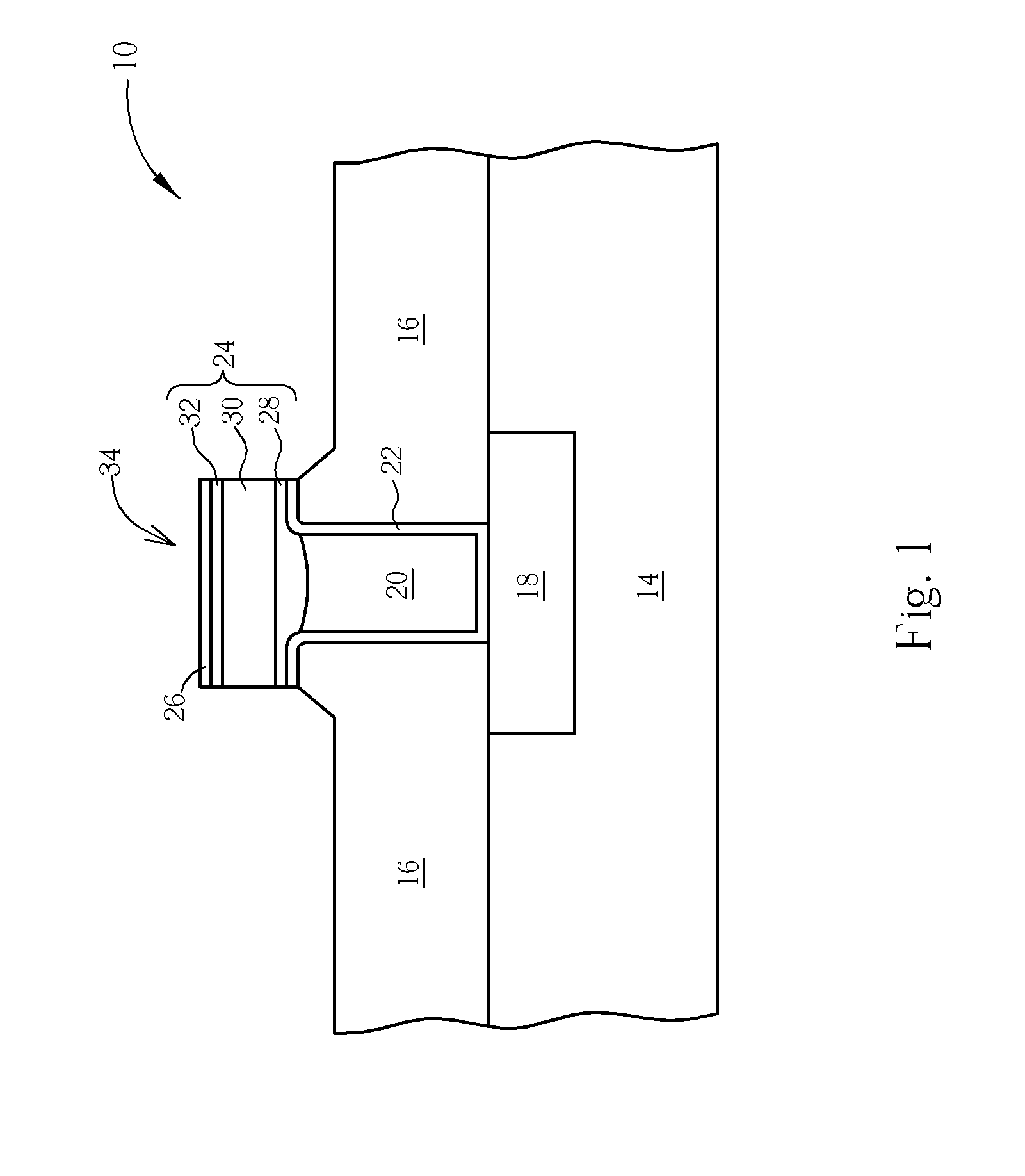
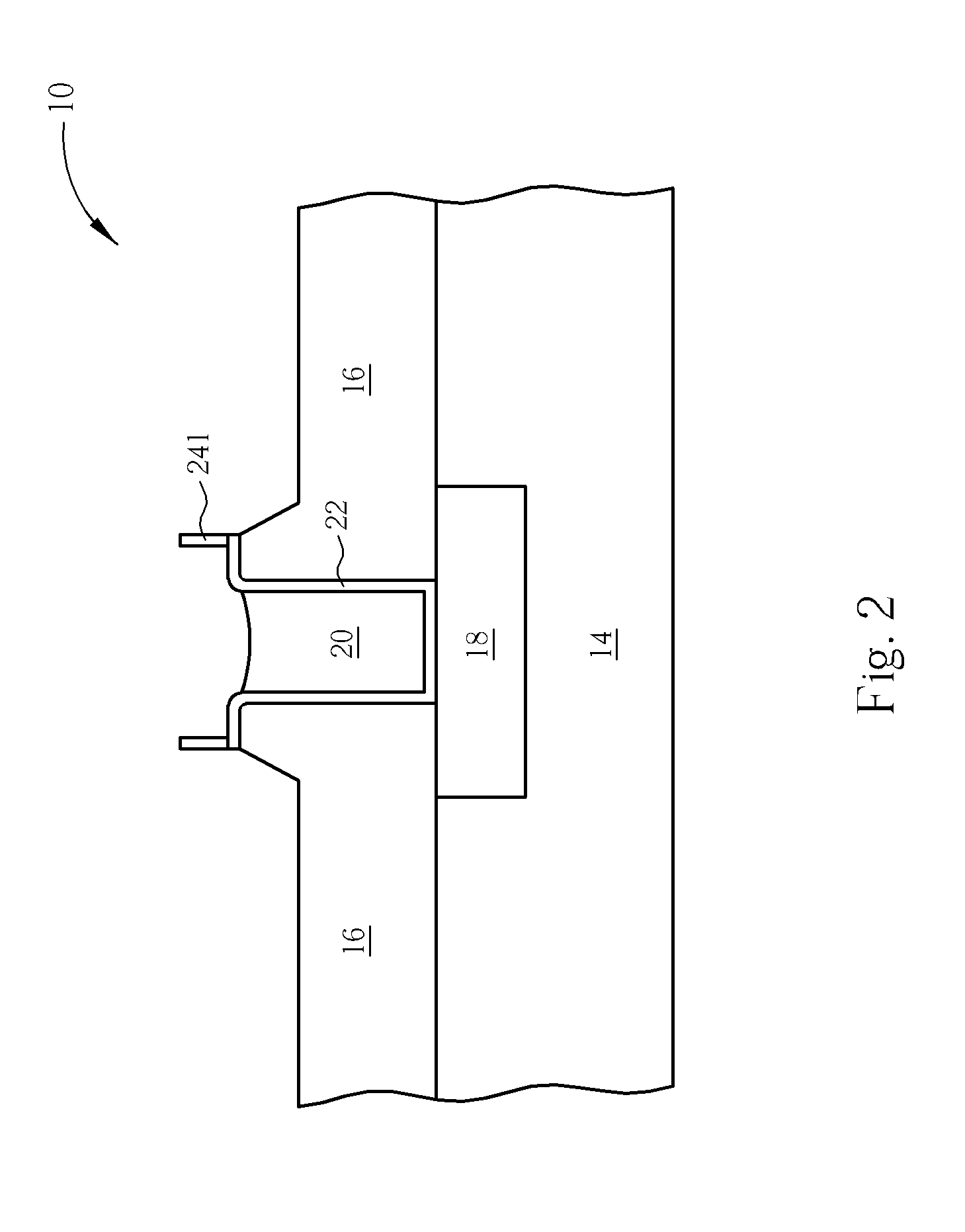
[0019]Please refer to FIG. 1-6, which are schematic diagrams illustrating a reworking method to remove defects on an integrated circuit device according to a first preferred embodiment of the present invention. An integrated circuit device 10 is provided. The integrated circuit device 10 includes a substrate 14 and a dielectric layer 16. The integrated circuit device 10 also has a conductive material layer 18 embedded in the substrate 14. A contact plug 20 is formed in the dielectric layer 16, and the contact plug 20 is electrically connected to the conductive material layer 18. A barrier layer 22, a first cond...


PUM


Abstract

Reworking method for removing defects on integrated circuit device is disclosed. An integrated circuit is provided, which has a substrate, a conductive material layer formed in the substrate, a dielectric layer formed on the substrate, at least a contact plug embedded in the dielectric layer, and a conductive layer contacting to the contact plug formed on the dielectric layer. A defect is found in the conductive layer and the reworking method is performed, including an etch back process, a chemical mechanical polishing process, and a deposition process. The reworking method removes the prior formed conductive layer and reform a conductive layer to prevent the integrated circuit from being scraped.

Description

BACKGROUND OF THE INVENTION[0001]1. Field of the Invention[0002]The present invention is related to a reworking method for removing defects on integrated circuit devices, and particularly, to a reworking method for removing defects on the conductive layer of a metal interconnection and for rebuilding the conductive layer to reduce the scrape rate of the integrated circuit device.[0003]2. Description of the Prior Art[0004]Integrated circuit devices have a tendency toward higher density and higher integration. In recent years, integrated circuit devices are formed as multi-layered metal interconnections for increasing the electrical connections between the metal interconnections themselves or between the integrated circuit devices and the metal interconnections. The fabrication process of the integrated circuit devices is very complicated. Integrated circuit devices are typically fabricated after gone through hundreds of different processing steps. For example, during the process of t...

Claims


Application Information

Patent Timeline
Patent Type & Authority Patents(United States)
IPC IPC(8): H01L21/00H01L29/40
CPCH01L21/02079H01L21/7685H01L21/76886H01L23/5226H01L23/53223H01L2924/0002H01L23/53238H01L23/53266H01L2924/00
Inventor SHIH, HUI-SHEN
Owner UNITED MICROELECTRONICS CORP
Why Eureka
Try Eureka