P-channel power MIS field effect transistor and switching circuit

a technology of switching circuit, which is applied in the direction of basic electric elements, electrical equipment, semiconductor devices, etc., can solve the problems of not only mos transistors, power mis field effect transistors with the same size, and no practical p-channel power mis field effect transistors having current drivability equal, etc., to achieve improved current drivability, improved current drivability, and improved silicon surface having substantially a (110) plane

Inactive Publication Date: 2010-02-16
OHMI TADAHIRO +1
View PDF17 Cites 31 Cited by
  • Summary
  • Abstract
  • Description
  • Claims
  • Application Information

AI Technical Summary

Benefits of technology

[0054]In the present invention, in a P-channel power MIS field effect transistor which includes a substrate having a silicon region whose surface is substantially a (110) plane, a gate insulation film formed on the surface, and a gate electrode formed on the gate insulation film, and in which the silicon region is used at least as a channel, at least a contact portion of the gate insulation film, which is in contact with the surface of the silicon region, contains argon, krypton, or xenon. This makes it possible to obtain a P-channel power MIS field effect transistor having current drivability equal to or higher than that of an N-channel MOS transistor for the same size, which cannot be achieved or implemented by either a (100) plane or (110) plane by the conventional method.
[0055]In addition, in the present invention, the flatness of the silicon surface having substantially a (110) plane is improved from a surface roughness (Ra) of about 1.0 nm, which is obtained by the conventional RCA cleaning, to 0.15 nm or less. Consequently, the current drivability can be improved by about three times from that of a MIS transistor formed by using the conventional RCA cleaning. Accordingly, the P-channel power MIS field effect transistor of the present invention can have current drivability equal to or higher than that of an N-channel power MIS field effect transistor for the same size and the same cost. Furthermore, in the present invention, the reliability of the gate insulation film can also be improved because the interface between the silicon surface and gate insulation film is atomically flat.

Problems solved by technology

As described above, it is proposed to form a P-channel power MIS field effect transistor on a (110) plane of silicon, but no practical P-channel power MIS field effect transistor having current drivability equal to or higher than that of an N-channel power MOS field effect transistor for the same size has been implemented.
Note that the above problem arises not only in MOS transistors but also in general MIS transistors having gate insulation films.

Method used


Image

  • P-channel power MIS field effect transistor and switching circuit
  • P-channel power MIS field effect transistor and switching circuit
  • P-channel power MIS field effect transistor and switching circuit

Examples


first embodiment

[0079]An embodiment of the present invention will be explained in detail below. In this embodiment, a P-channel power MIS field effect transistor in which a gate insulation film made of a silicon oxide film is formed on a silicon substrate having a (110) plane on its surface will be described.

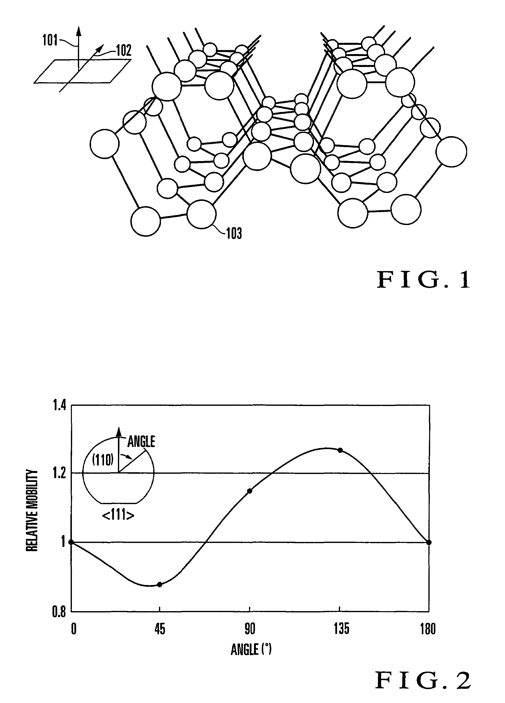
[0080]FIG. 1 is a schematic view showing the crystal structure viewed in the direction of a silicon crystal forming the silicon substrate used in the field effect transistor of this embodiment. Referring to FIG. 1, each of arrows 101 and 102 indicates the direction, showing that silicon atoms 103 are arranged parallel to the interface with the gate insulation film on the substrate uppermost surface on which the field effect transistor is formed.

[0081]In addition, in the field effect transistor of this embodiment, a gate electrode is formed on the major surface of the silicon substrate, e.g., a (110) plane, such that the longitudinal direction of the gate electrode extends in the horizontal d...

third embodiment

[0122]As the third embodiment of the present invention, a P-channel power MIS field effect transistor in which a gate insulation film made of a silicon nitride film is formed on a silicon substrate having a (110) plane on its surface will be described below.

[0123]Even when a field effect transistor using a silicon nitride film as a gate insulation film is to be formed, the highest mobility is given by the arrangement shown in FIG. 1 in which on a silicon substrate, silicon atoms on the uppermost surface are arranged parallel to the interface with the gate insulation film, a gate electrode is formed such that its longitudinal direction is the horizontal direction of the paper, and a source region and drain region are formed forward and backward, respectively, with respect to the paper.

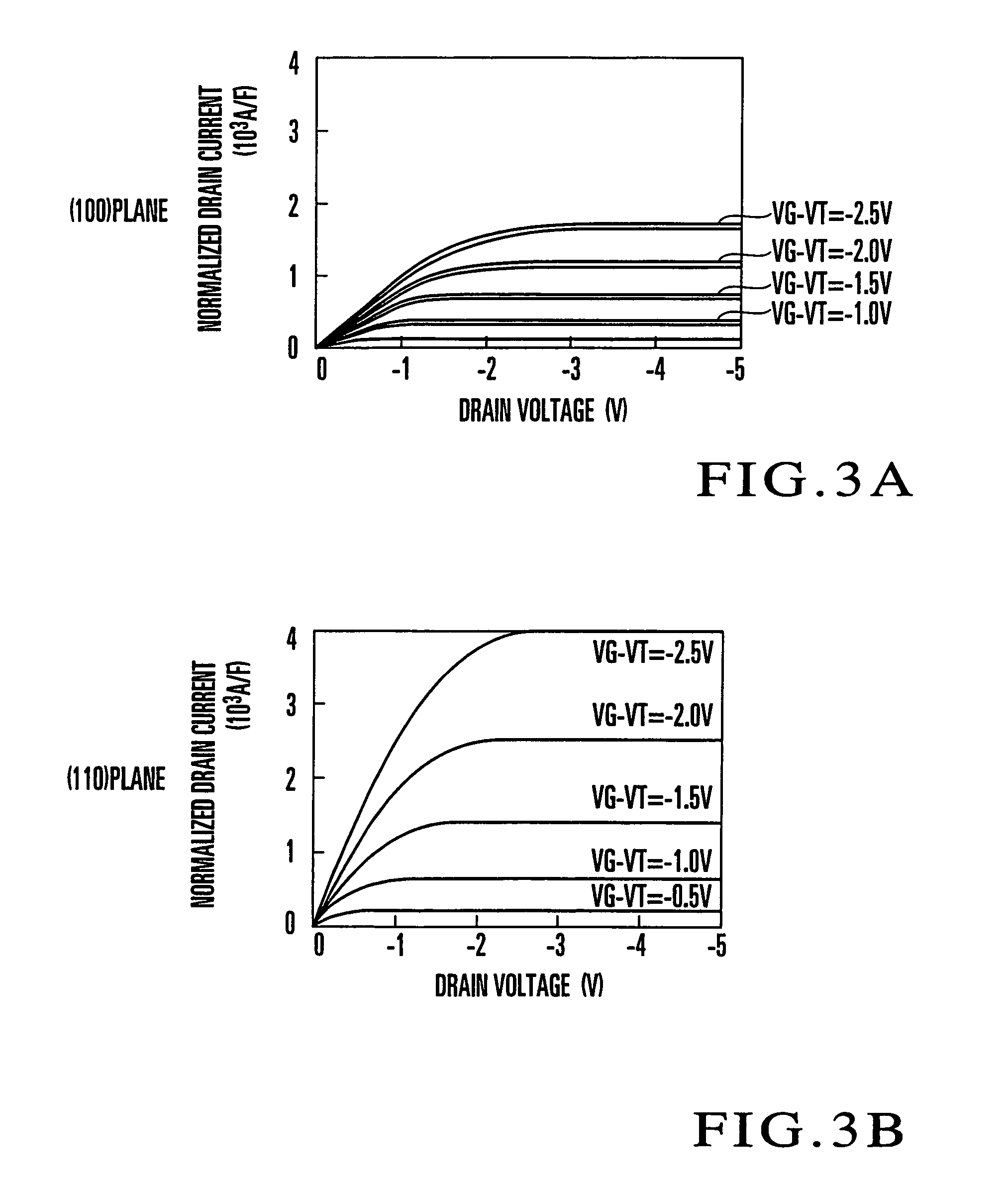
[0124]The current drivability of the MIS field effect transistor of this embodiment formed in this direction is higher than that of the first embodiment by an amount in which the dielectric constant of...

fourth embodiment

[0135]The fourth embodiment of the present invention in which the characteristics of a P-channel power MIS field effect transistor are improved by reducing the roughness of a silicon surface will be explained below.

[0136]The present inventors have found by observation that when a field effect transistor is fabricated, the surface of an element region is inevitably roughened by, e.g., an alkali treatment and pure water rinsing during RCA cleaning.

[0137]On the other hand, the mobility of carriers in a field effect transistor is an index of the current drivability of the transistor, and holes are carriers in a P-channel field effect transistor. Generally, to improve the current drivability of a field effect transistor, the carrier mobility must be increased by decreasing the roughness of the surface of an element region.

[0138]More specifically, the present inventors have confirmed that when normal RCA cleaning is used, the surface roughness of silicon in an element region is about 0.5 ...


PUM


Abstract

In a P-channel power MIS field effect transistor formed on a silicon surface having substantially a (110) plane, a gate insulation film is used which provides a gate-to-source breakdown voltage of 10 V or more, and planarizes the silicon surface, or contains Kr, Ar, or Xe.

Description

RELATED APPLICATIONS[0001]This application is a continuation under 35 U.S.C. 111(a) of PCT / JP2004 / 007075, filed May 24, 2004, and published on Dec. 2, 2004 as WO 2004 / 105116 A1, which claimed priority to Japanese Application No. 148275 / 2003, filed May 26, 2003, which applications and publication are incorporated herein by reference.TECHNICAL FIELD[0002]The present invention relates to a P-channel power MIS field effect transistor, and more particularly to a P-channel power MIS field effect transistor by which performance equal to or higher than that of an N-channel power MIS field effect transistor can be obtained for the same size and the same cost, and a switching circuit using this P-channel power MIS field effect transistor.BACKGROUND ART[0003]To move and stop automobile electronic parts such as wipers and door locks, switching circuits which turn on / off voltage supply from batteries to loads such as motors are used. Although relays are conventionally used as these switching cir...

Claims


Application Information

Patent Timeline
Patent Type & Authority Patents(United States)
IPC IPC(8): H01L29/76H01L21/316H01L21/28H01L21/318H01L29/04H01L29/51H01L29/78
CPCH01L21/28211H01L29/045H01L29/66734H01L29/7813H01L21/28194H01L21/28202H01L29/513H01L29/517H01L29/518H01L21/18
Inventor OHMITERAMOTO, AKINOBUAKAHORI, HIROSHINII, KEIICHIWATANABE, TAKANORI
Owner OHMI TADAHIRO
Why Eureka
Try Eureka