Module and mounted structure using the same

a module and mounting technology, applied in the direction of printed circuit aspects, electrical apparatus construction details, printed circuit non-printed electric components association, etc., can solve the problems of increasing the cost of the substrate, becoming technologically difficult to solder the semiconductor chip, and poor versatility, so as to reduce the number of wirings, reduce the manufacturing cost of the module, and reduce the influence of nois

Inactive Publication Date: 2010-02-23
PANASONIC CORP
View PDF15 Cites 23 Cited by
  • Summary
  • Abstract
  • Description
  • Claims
  • Application Information

AI Technical Summary

Benefits of technology

[0011]The present invention provides a module that not only can achieve the reduction in size and manufacturing cost but also be impervious to noise due to electromagnetic waves, and a mounted structure using the same.
[0014]In accordance with the module of the present invention, each of the plurality of semiconductor packages includes a first radio communication element for transmitting and receiving a signal between the semiconductor chips in the plurality of semiconductor packages by radio communication, so that the number of wirings can be reduced. This makes it possible to provide a module that can be miniaturized. Also, since the first radio communication element is constituted independently of the semiconductor chip, existing products can be used for both of the first radio communication element and the semiconductor chip. This can reduce the manufacturing cost of the module. Furthermore, since the first radio communication element is constituted independently of the semiconductor chip, it is possible to reduce the influence of the noise due to electromagnetic waves on the semiconductor chip. Moreover, the mounted structure of the present invention includes the above-described module of the present invention, so that a mounted structure that can not only achieve the reduction in size and manufacturing cost but also be impervious to noise due to electromagnetic waves can be provided similarly to the above.

Problems solved by technology

Consequently, it has become technologically difficult to solder the semiconductor chip.
Also, since more layers of finer substrates on which the semiconductor chips are mounted are stacked, an increase in the cost of the substrates has become apparent.
Also, since an existing semiconductor chip cannot be used, the versatility is poor.

Method used


Image

  • Module and mounted structure using the same
  • Module and mounted structure using the same
  • Module and mounted structure using the same

Examples


embodiment 1

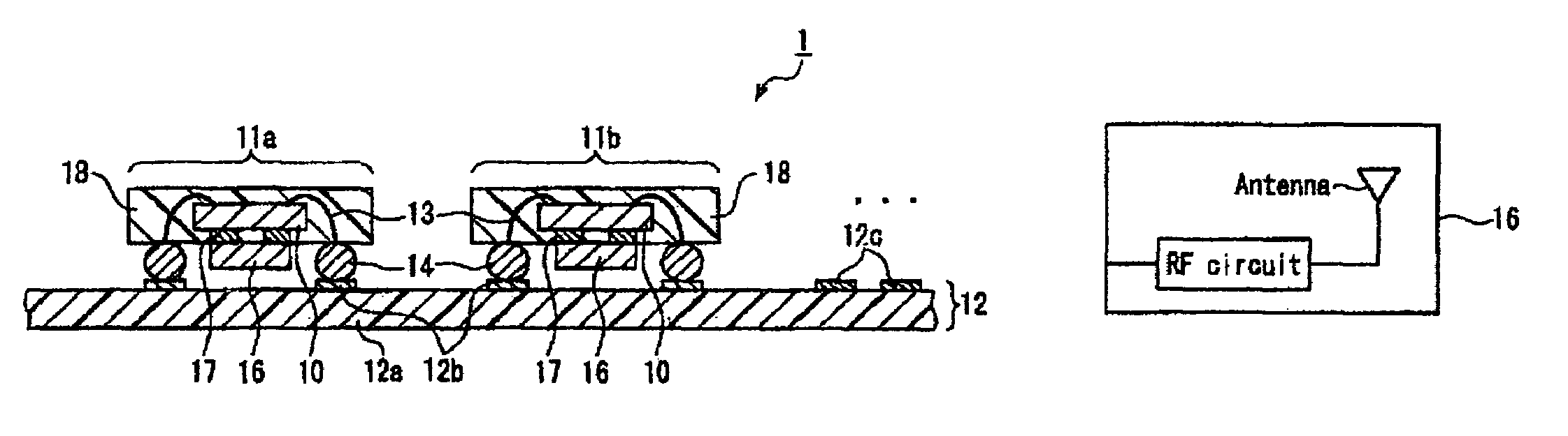
[0042]First, a module according to Embodiment 1 of the present invention will be described with reference to the accompanying drawings. FIG. 1A to be referred to is a schematic sectional view showing the module according to Embodiment 1. FIG. 2 to be referred to is a plan view, seen from a substrate side, schematically showing a semiconductor package included in the module according to Embodiment 1.

[0043]As shown in FIG. 1A, a module 1 according to Embodiment 1 has a substrate 12 and a plurality of semiconductor packages 11a, 11b . . . (in the following, simply referred to as “the semiconductor packages 11a, 11b”), each including a semiconductor chip 10, mounted on the substrate 12.

[0044]The semiconductor chip 10 is connected electrically to a terminal 12b formed on one principal surface of a base 12a constituting the substrate 12 via bonding wires 13 and electrically conductive portions 14 formed of solder or the like. It should be noted that the terminal 12b can be at least one te...

embodiment 2

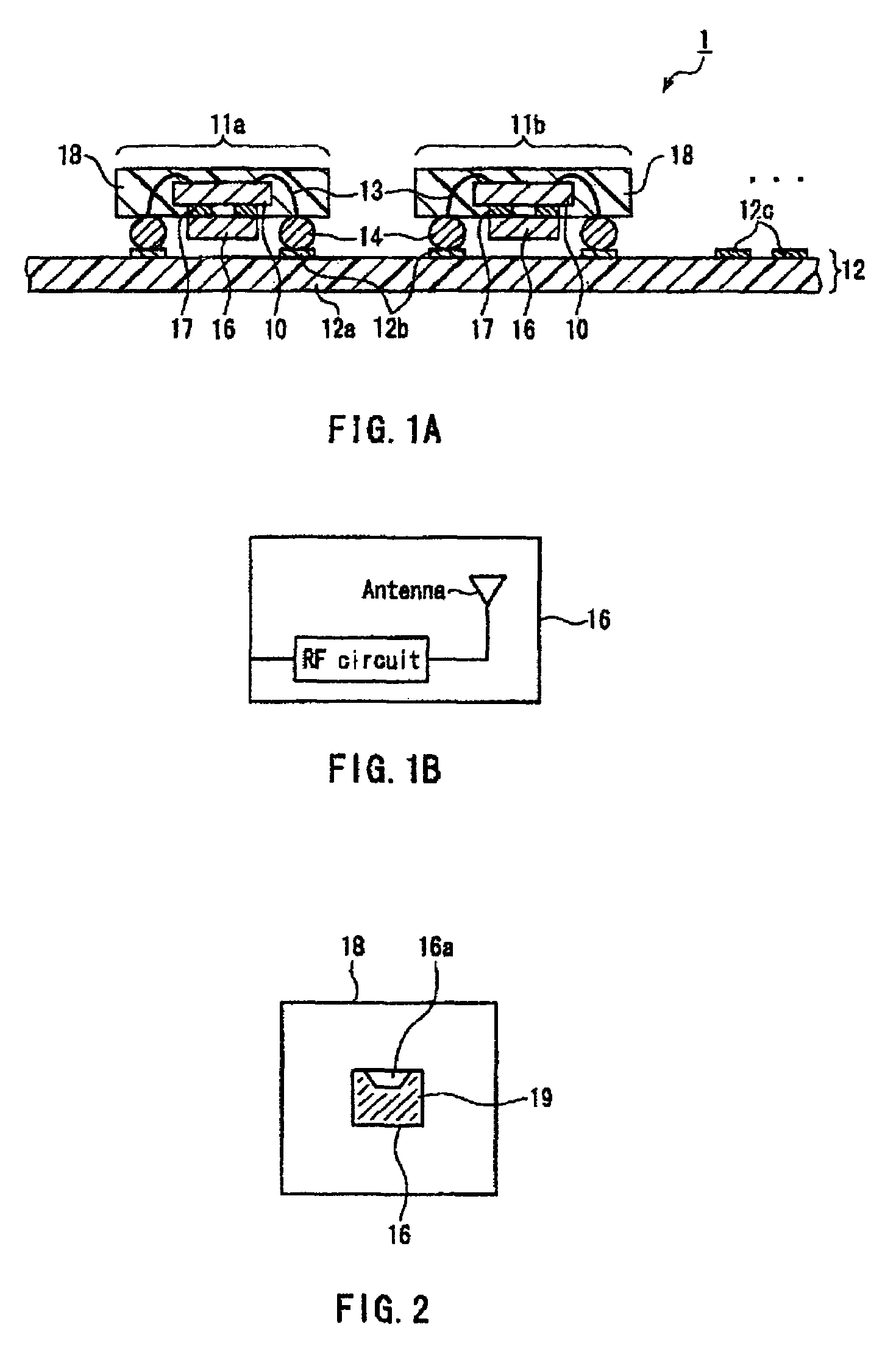
[0055]Next, a module according to Embodiment 2 of the present invention will be described with reference to the accompanying drawings. FIG. 3 to be referred to is a sectional view schematically showing the module according to Embodiment 2. Constituent elements that are the same as those in FIG. 1A are assigned the same reference signs, and the description thereof will be omitted.

[0056]As shown in FIG. 3, a module 2 according to Embodiment 2 has a substrate 12 and a plurality of semiconductor packages 21a, 21b . . . (in the following, simply referred to as “the semiconductor packages 21a, 21b”), each including a semiconductor chip 20, mounted on the substrate 12. Each of the semiconductor packages 21a, 21b further includes an interposer 22 on which the semiconductor chip 20 is placed.

[0057]The semiconductor chip 20 includes a semiconductor chip 20a and a semiconductor chip 20b stacked on the semiconductor chip 20a. The semiconductor chip 20a is mounted on the interposer 22 via electr...

embodiment 3

[0064]Next, a module according to Embodiment 3 of the present invention will be described with reference to the accompanying drawings. FIG. 5 to be referred to is a schematic sectional view showing the module according to Embodiment 3. Constituent elements that are the same as those in FIG. 3 are assigned the same reference signs, and the description thereof will be omitted.

[0065]As shown in FIG. 5, a module 3 according to Embodiment 3 includes a second radio communication element 30 for transmitting and receiving a signal by radio communication with respect to at least one of first radio communication elements 16 included respectively in semiconductor packages 21a, 21b, and an electronic component 31 that is connected electrically to the second radio communication element 30. The second radio communication element 30 is mounted on wirings 12c of a substrate 12 via electrically conductive portions 32 formed of an electrically conductive material such as copper or solder. The electro...


PUM


Abstract

A module that can not only achieve the reduction in size and manufacturing cost but also be impervious to noise due to electromagnetic waves, and a mounted structure using the same are provided. A module (1) includes a substrate (12) and a plurality of semiconductor packages (11a, 11b), each including a semiconductor chip (10), mounted on the substrate (12). Each of the plurality of semiconductor packages (11a, 11b) includes a first radio communication element (16) for transmitting and receiving a signal between the semiconductor chips (10) in the plurality of semiconductor packages (11a, 11b) by radio communication, and the first radio communication element (16) is constituted independently of the semiconductor chip (10).

Description

TECHNICAL FIELD[0001]The present invention relates to a module including a plurality of semiconductor packages and a mounted structure using the same.BACKGROUND ART[0002]Accompanying the miniaturization and performance enhancement of electronic equipment in recent years, a larger number of pins are included in a semiconductor chip of the electronic equipment, and smaller electronic components of various types constitute the electronic equipment. Accordingly, there has been a dramatic increase in the number and density of wirings in a substrate on which these chips and components are mounted. In particular, the number of terminals in the semiconductor chip and the number of leads led out from the semiconductor chip have increased rapidly, thus narrowing the terminal pitch of the semiconductor chip and the wiring pitch of the substrate on which the semiconductor chip is mounted (a printed board). Consequently, it has become technologically difficult to solder the semiconductor chip. A...

Claims


Application Information

Patent Timeline
Patent Type & Authority Patents(United States)
IPC IPC(8): H05K7/02H05K7/06H05K7/08H05K7/10H01L23/31H01L25/04H01L25/065H01L25/10H01L25/18H05K1/02H05K1/18
CPCH05K1/02H01L23/66H01L25/0657H01L25/18H01L2224/16225H01L2224/48091H01L2224/48225H01L2224/73204H01L2225/06558H01L2924/01078H01L2924/01079H01L2924/15311H01L2924/1532H01L2924/19041H01L2924/19105H01L2924/19106H01L2924/3025H05K1/181H05K2201/10098H01L2924/00014H01L23/3128H01L23/552H01L25/105H01L24/48H01L2225/1023H01L2225/107H01L2225/1005H01L2223/6677H01L2225/0651H01L2225/06517H05K2201/1053H01L2224/48227H01L2224/16227H01L2224/32145H01L2224/32225H01L2224/73207H01L2224/73253H01L2224/73265H01L2924/19104H01L2924/14H01L2924/00011H01L2924/00012H01L2924/00H01L2224/0401H01L2224/45099H01L2224/45015H01L2924/207
Inventor NAKATANI, SEIICHIMITANI, TSUTOMU
Owner PANASONIC CORP
Why Eureka
Try Eureka