Solid-state imaging device, signal charge detection device, and camera

a solid-state imaging and detection device technology, applied in semiconductor devices, radio frequency controlled devices, electrical apparatuses, etc., can solve the problems of reducing the efficiency of electric charge to voltage conversion is not satisfactory, and the above-conventional technology has various problems, so as to increase the accuracy of the dimension of the first wire, reduce the stray capacitance of the first wire itself, and increase the efficiency of charge-to-voltage conversion

Inactive Publication Date: 2010-03-02
COLLABO INNOVATIONS INC
View PDF7 Cites 4 Cited by
  • Summary
  • Abstract
  • Description
  • Claims
  • Application Information

AI Technical Summary

Benefits of technology

[0014]An object of the present invention is to provide a solid-state imaging device, a signal charge detection device, and a camera, in which the efficiency of charge-to-voltage conversion is increased, and the S / N rate and the sensibility are also increased.
[0036]Furthermore, it is possible to increase reliability, and particularly to prevent characteristic degradation affected by air humidity.FURTHER INFORMATION ABOUT TECHNICAL BACKGROUND TO THIS APPLICATION

Problems solved by technology

However, the above conventional technologies have various problems.
The first problem is that efficiency of conversion from electric charge to a voltage (hereinafter, referred to also as “charge-to-voltage conversion”) is not satisfactory.
As a result, a stray capacitance (parasitic capacitance) among the wire 205 and the semiconductor substrate and the like damages the signal charges held in the floating diffusion region 201, which results in reduction of the efficiency of charge-to-voltage conversion.
The second problem is that the S / N rate and the sensitivity of the output voltage are varied.

Method used


Image

  • Solid-state imaging device, signal charge detection device, and camera
  • Solid-state imaging device, signal charge detection device, and camera
  • Solid-state imaging device, signal charge detection device, and camera

Examples


first embodiment

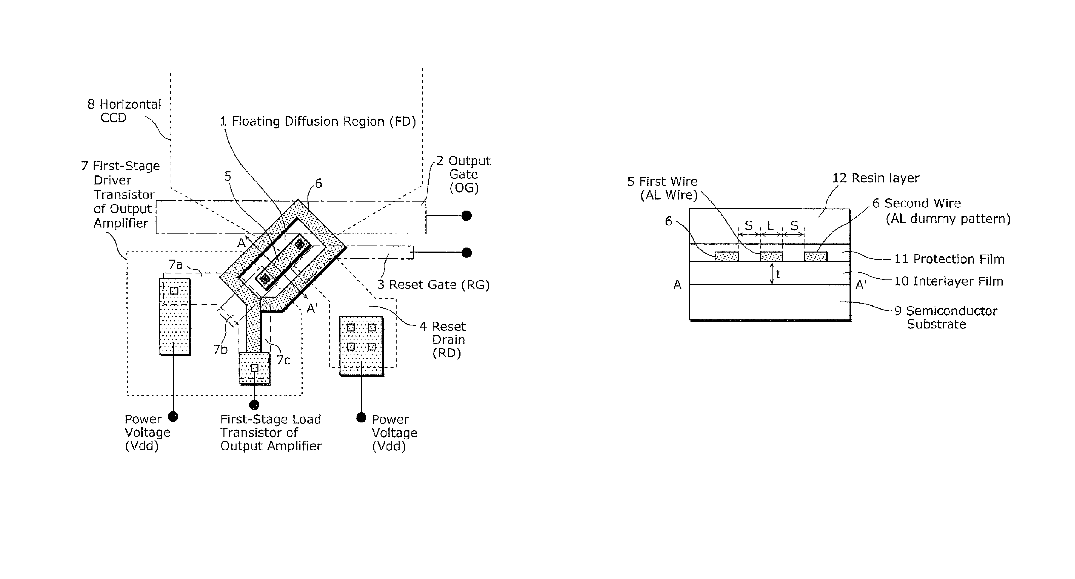
[0053]The first embodiment is characterized by having: the first wire which connects (i) a floating diffusion region (floating diffusion capacity unit) which is formed at a final stage of a horizontal CCD with (ii) an input of an amplifier which converts signal charges to a voltage; and the second wire which is made of the same material as the first wire, formed in the same layer as the first wire, arranged around all sides of the first wire, and electrically insulated from the first wire. The following describes a solid-state imaging device having the above structure, by which accuracy of a finished dimension of the first wire is increased, and eventually the area (length by width) of the first wire conforms with the design rule and becomes smaller than the area of the corresponding wire in the conventional solid-state imaging device.

[0054]The solid-state imaging device according to the first embodiment is described herein below with reference to FIGS. 4 to 7. Firstly, a schematic ...

second embodiment

[0070]In the first embodiment, the second wire 6 is overlapped with the reset gate 3, which would affect resetting of the floating diffusion region. In order to eliminate such affecting, in the second embodiment which will be described herein, the second wire is arranged around the first wire but not on a part which is overlapped with at least a part of the reset gate 3.

[0071]FIG. 8 is an enlarged plane view showing a final stage of a horizontal CCD of a CCD solid-state imaging device according to the second embodiment of the present invention. The structure shown in FIG. 8 differs from the structure shown in FIG. 5 in that the second wire 6 is replaced by the second wire 6a. Note that the structure of the second embodiment is the same as the structure of the first embodiment except the above difference, so that the same aspects are not described again and the following mainly describes the difference.

[0072]The second wire 6a of FIG. 8 differs from the second wire 6 of FIG. 5 in tha...

third embodiment

[0075]In the first embodiment, the width of the second wire 6 is greater than the width of the second wire 5. In the third embodiment, however, a solid-state imaging device is described to increase accuracy of finished dimension of the second wire, thereby further increasing accuracy of finished dimension of the first wire.

[0076]FIG. 9 is an enlarged plane view showing a final stage of a horizontal CCD of a CCD solid-state imaging device according to the third embodiment of the present invention. The structure of the FIG. 9 differs from the structure shown in FIG. 5 in that a plurality of the third wires 16 are further added. Note that the structure of the third embodiment is the same as the structure of the first embodiment except the above difference, so that the same aspects are not described again and the following mainly describes the difference.

[0077]Each of the third wires 16 is made of the same material as the second wire 6, formed in the same layer as the second wire 6, arr...


PUM


Abstract

The solid-state imaging device of the present invention includes: a floating diffusion capacity unit which is formed on a semiconductor substrate, and is operable to hold signal charges derived from incident light; an amplifier which is operable to convert the signal charges held in the floating diffusion capacity unit into a voltage; the first wire which connects the floating diffusion capacity unit to an input of the amplifier; and a second wire which is made of the same material as the first wire, formed in the same layer as the first wire, arranged around the first wire at least along long sides of the first wire, and electrically insulated from the first wire.

Description

BACKGROUND OF THE INVENTION[0001](1) Field of the Invention[0002]The present invention relates to a solid-state imaging device, and more particularly to a Charge Coupled Device (CCD) solid-state imaging device, a signal charge detection device, and a camera.[0003](2) Description of the Related Art[0004]In recent years, there has been increasing demand for solid-state imaging devices as imaging devices in digital still cameras, digital video cameras, and the like. Further, portable terminal devices represented by a portable telephone are required to have a camera function, so that the demand for the solid-state imaging device has also been growing for imaging devices in such portable terminal devices. Furthermore, with the aim of realizing high-resolution image, the number of pixels in the solid-state imaging device tends to be increased year by year. Still further, with the requirement for high sensitivity of the digital still cameras, the digital video cameras, the portable termina...

Claims


Application Information

Patent Timeline
Patent Type & Authority Patents(United States)
IPC IPC(8): H01L27/148
CPCH01L27/14831H01L29/76816H01L2924/0002H01L2924/00
Inventor KURIYAMA, TOSHIHIRO
Owner COLLABO INNOVATIONS INC
Why Eureka
Try Eureka