Wide gap semiconductor power device with temperature independent resistivity due to channel region resistivity having negative temperature dependence

a wide-band gap semiconductor and resistivity technology, which is applied in the direction of transistors, force measurement, instruments, etc., can solve the problems of no longer functioning as a current controlling device, the operation of a system controlled by that circuit becomes unstable, and the device characteristics change, so as to reduce the change in the resistance of the device to the temperature, the effect of high temperature stability and high reliability

Active Publication Date: 2010-03-02
PANASONIC CORP
View PDF12 Cites 18 Cited by
  • Summary
  • Abstract
  • Description
  • Claims
  • Application Information

AI Technical Summary

Benefits of technology

[0027]According to the present invention, there is provided a power device which is highly stable against temperature, and which undergoes a reduced change in its ON resistance against device temperature. It is advantageous to construct a power electronics circuit (e.g., an inverter circuit) by using such a power device because it is not necessary to provide any superfluous circuitry for feedback control. Therefore, there is provided a highly reliable power electronics circuit having a simple structure, whose feedback circuit is simplified or omitted, and which realizes a stable operation of a system. Furthermore, a highly reliable power electronics system incorporating such a power electronics circuit can be realized.

Problems solved by technology

A power device has a problem in that the temperature of the power device increases due to power losses, which causes changes in its device characteristics.
A power device utilizing a silicon semiconductor (Si power device) which has a band gap of about 1.11 eV at room temperature undergoes a thermal runaway at temperatures over 150° C. and thus is short-circuited, no longer functioning as a current controlling device.
However, there exists a problem in that, even if the temperature of a power device is maintained at or below a safe operating temperature (150° C.
Thus, when a current flowing through a load of a circuit exhibits temperature dependence, there is a problem in that the operation of a system which is controlled by that circuit becomes unstable.
However, the circuit structure would be complicated and the manufacturing cost would increase with the provision of such a feedback control.
Si power devices other than Si-MOSFETs also permit their electrical characteristics to change with temperature, and have similar problems to the above.

Method used


Image

  • Wide gap semiconductor power device with temperature independent resistivity due to channel region resistivity having negative temperature dependence
  • Wide gap semiconductor power device with temperature independent resistivity due to channel region resistivity having negative temperature dependence
  • Wide gap semiconductor power device with temperature independent resistivity due to channel region resistivity having negative temperature dependence

Examples


Embodiment Construction

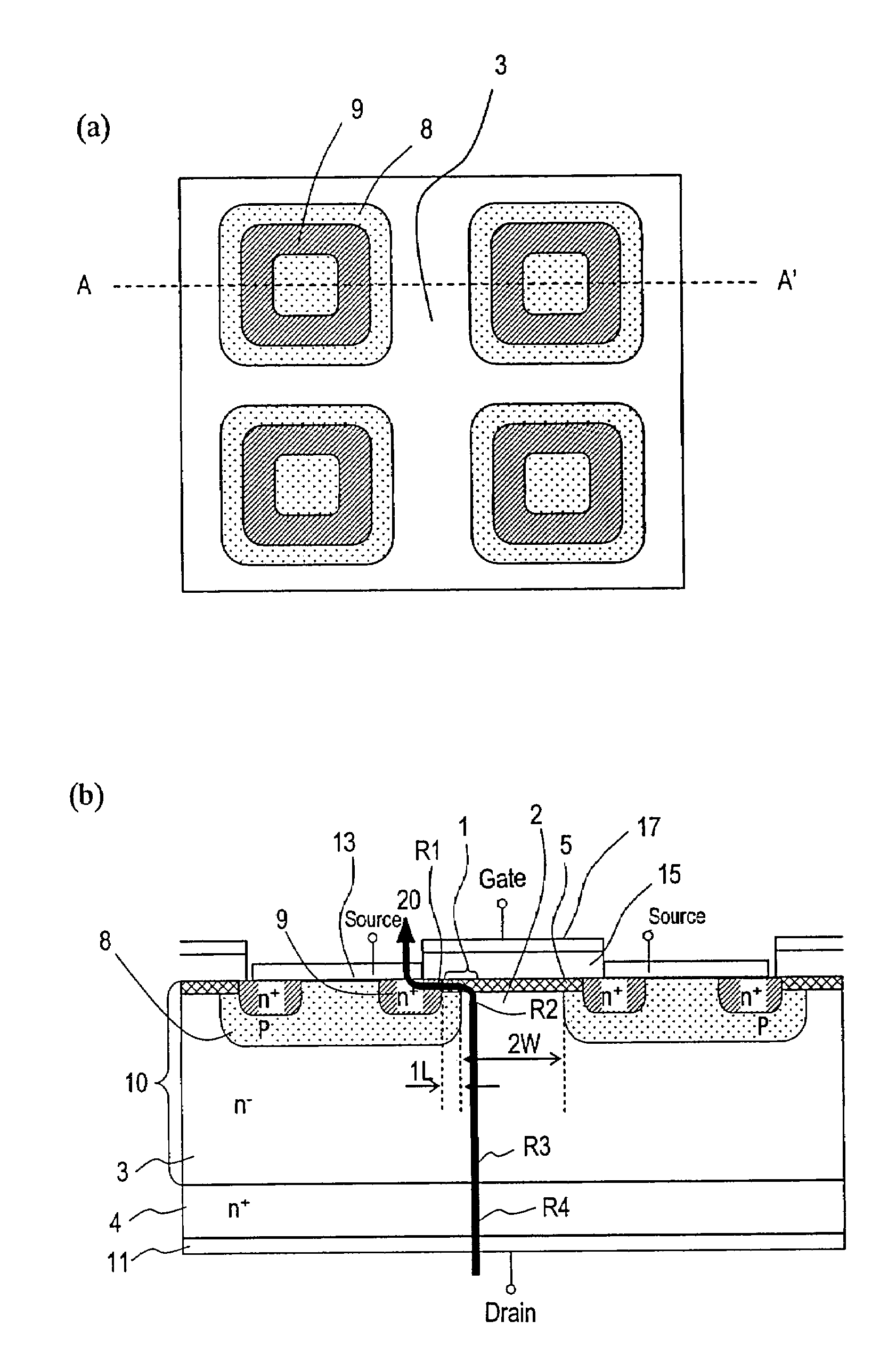
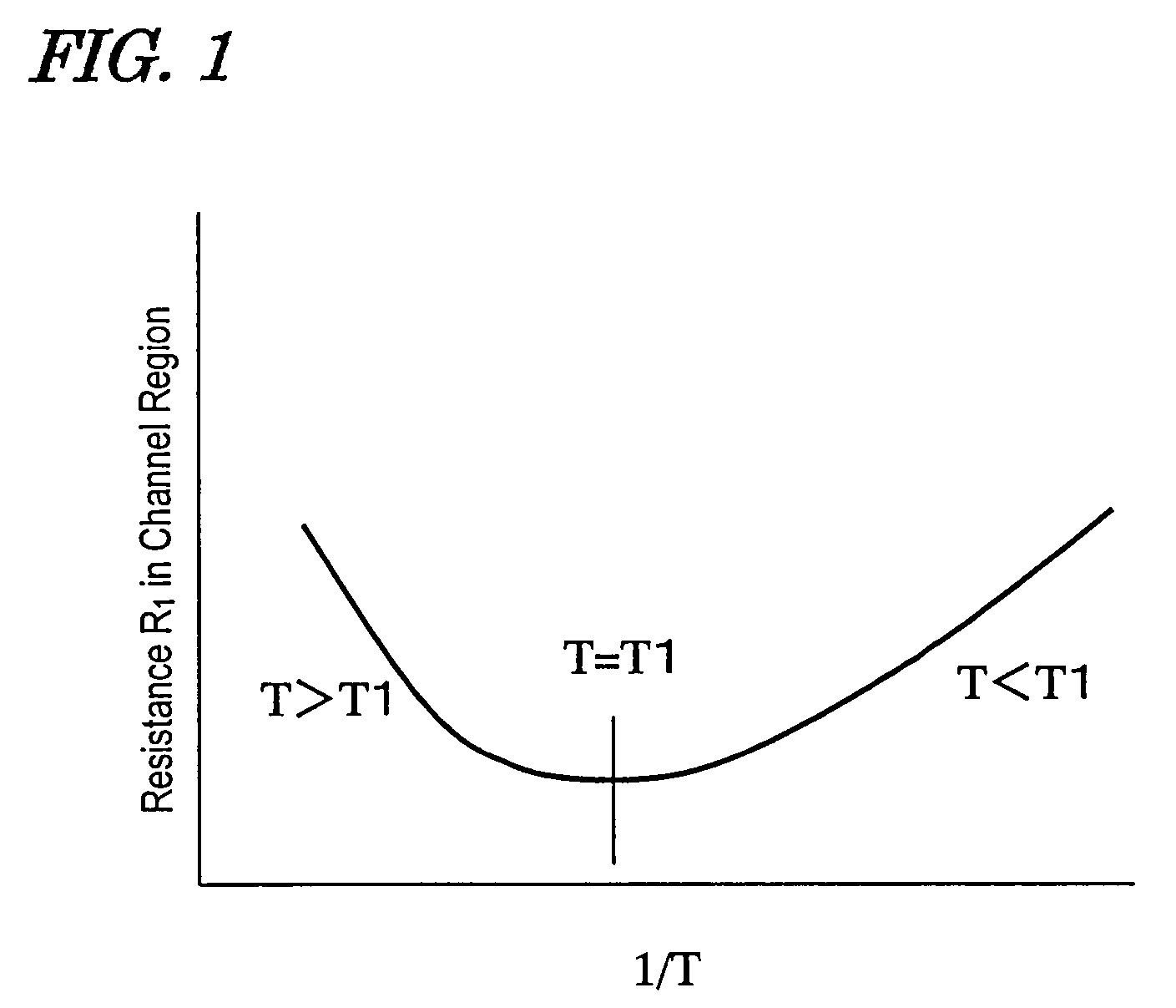
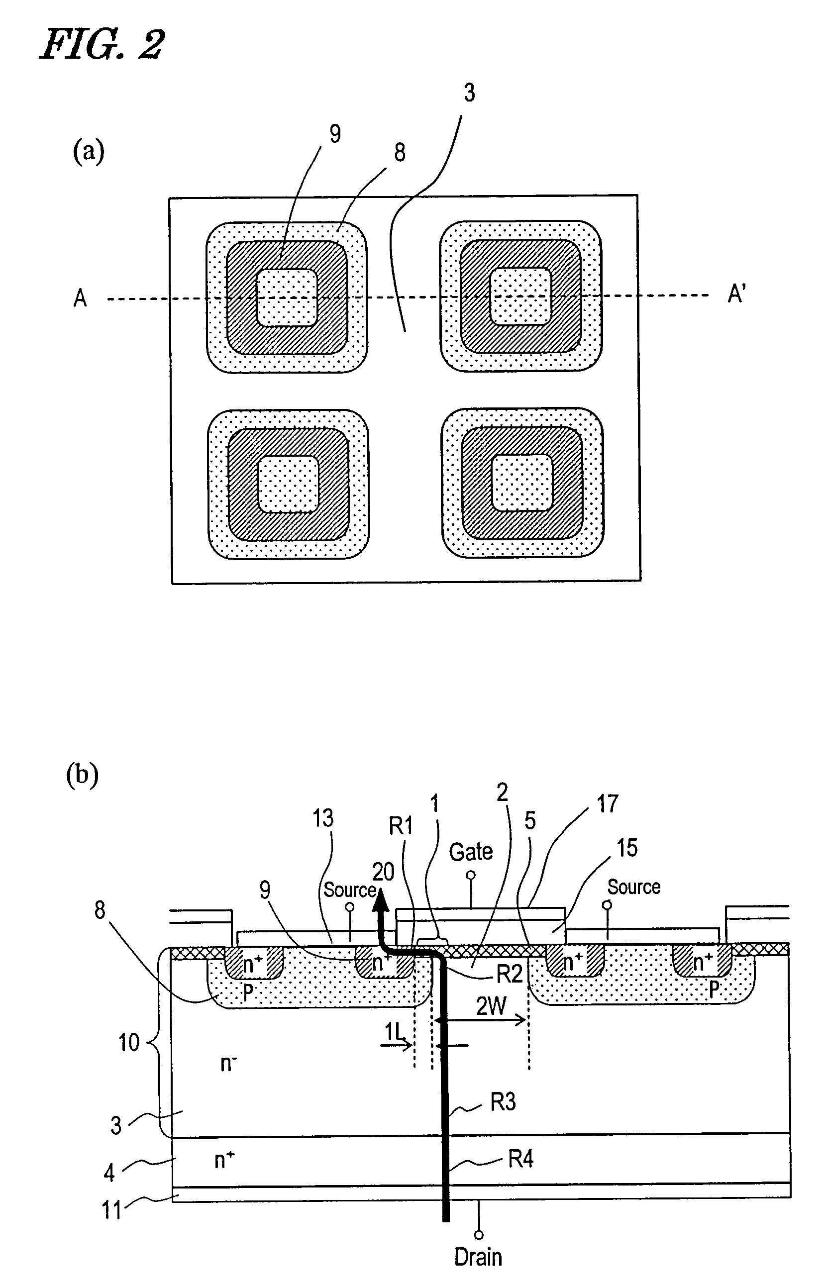
[0044]A power device according to the present invention has: a portion whose electrical resistance in a conducting state decreases at a desired rate responsive to a temperature increase (a channel region); and a portion whose electrical resistance in a conducting state increases at a desired rate responsive to a temperature increase (a region which is in series connection with the channel region). By allowing the changes in electrical resistance of these portions to cancel out each other, it is ensured that, with respect to the electrical resistance in a conducting state of the entire power device at −30° C., the amount of change in the electrical resistance in a conducting state at 100° C. is 50% or less. Such a power device is formed by using a wide gap semiconductor, such as silicon carbide (SiC). In the present specification, a “power device” refers to a semiconductor device which has a breakdown voltage of 100 V or more and which controls a current of 1 A or more.

[0045]In accor...


PUM


Abstract

A field-effect transistor power device includes a source electrode, a drain electrode, a wide gap semiconductor including a channel region and a drift region, the channel region and the drift region forming a series current path between the source electrode and the drain electrode, a gate insulating film that covers the channel region, and a gate electrode formed on the gate insulating film. In the series current path which is electrically conducting when the field-effect transistor power device is in an ON state, any region other than the channel region has an ON resistance exhibiting a positive temperature dependence, and the channel region has an ON resistance exhibiting a negative temperature dependence. A ratio ΔRon / Ron(−30° C.) is 50% or less.

Description

TECHNICAL FIELD[0001]The present invention relates to a power device utilizing a wide band gap semiconductor.BACKGROUND ART[0002]Power devices having a high breakdown voltage and a large current capability are used in various fields. A power device has a problem in that the temperature of the power device increases due to power losses, which causes changes in its device characteristics. In order to reduce such changes in the device characteristics, a structure has conventionally been adopted which cools the power device so as to be retained at or below a safe operating temperature. Specifically, the power device is kept in contact with a package base-material, and the heat generated in the power device is allowed to pass into the package base-material, thus minimizing increase in the device temperature.[0003]A power device utilizing a silicon semiconductor (Si power device) which has a band gap of about 1.11 eV at room temperature undergoes a thermal runaway at temperatures over 150...

Claims


Application Information

Patent Timeline
Patent Type & Authority Patents(United States)
IPC IPC(8): H01L29/24H01L29/06H01L29/78H01L29/80H01L29/808
CPCH01L29/7828H01L29/0696H01L29/0847H01L29/105H01L29/1608H01L29/365
Inventor KITABATAKE, MAKOTOKUSUMOTO, OSAMUUCHIDA, MASAOTAKAHASHI, KUNIMASAYAMASHITA, KENYAHASHIMOTO, KOICHI
Owner PANASONIC CORP
Why Eureka
Try Eureka