Semiconductor device

a technology of semiconductors and devices, applied in the field of semiconductor devices, can solve the problems of large scale, large power consumption, and inability to accurately obtain data from the carrier, and achieve the effects of reducing power consumption, small scale, and simplifying circuit configuration

Inactive Publication Date: 2010-03-09
SEMICON ENERGY LAB CO LTD
View PDF10 Cites 9 Cited by
  • Summary
  • Abstract
  • Description
  • Claims
  • Application Information

AI Technical Summary

Benefits of technology

[0015]In view of the foregoing, the invention provides a semiconductor device that generates a clock signal with a fixed pulse width from a carrier. The invention also provides a semiconductor device that can accurately obtain data from a carrier using a clock signal with a fixed pulse width.
[0025]According to the invention, the semiconductor device generates a clock signal using a signal obtained by dividing a carrier by a divider circuit and a demodulated signal outputted from a demodulated signal separation circuit, thereby a clock signal with a fixed pulse width can be generated. The clock signal with a fixed pulse width allows data to be obtained from a carrier accurately. In addition, the semiconductor device of the invention has a simpler circuit configuration and a smaller scale as compared to the PLL circuit; thus the power consumption can be reduced.

Problems solved by technology

When generating a clock signal from a carrier including 100% modulation, however, the pulse width thereof may not be fixed but may be longer than a predetermined width in a portion.
When using such a clock signal with a variable pulse width, 100% modulated position of a carrier cannot be read accurately, which makes it impossible to accurately obtain data from the carrier.
The PLL circuit is generally complicated, large in scale, and consumes much power; therefore, it is not suitable to be incorporated in a semiconductor device having limited power supply.

Method used


Image

  • Semiconductor device
  • Semiconductor device
  • Semiconductor device

Examples


embodiment mode 1

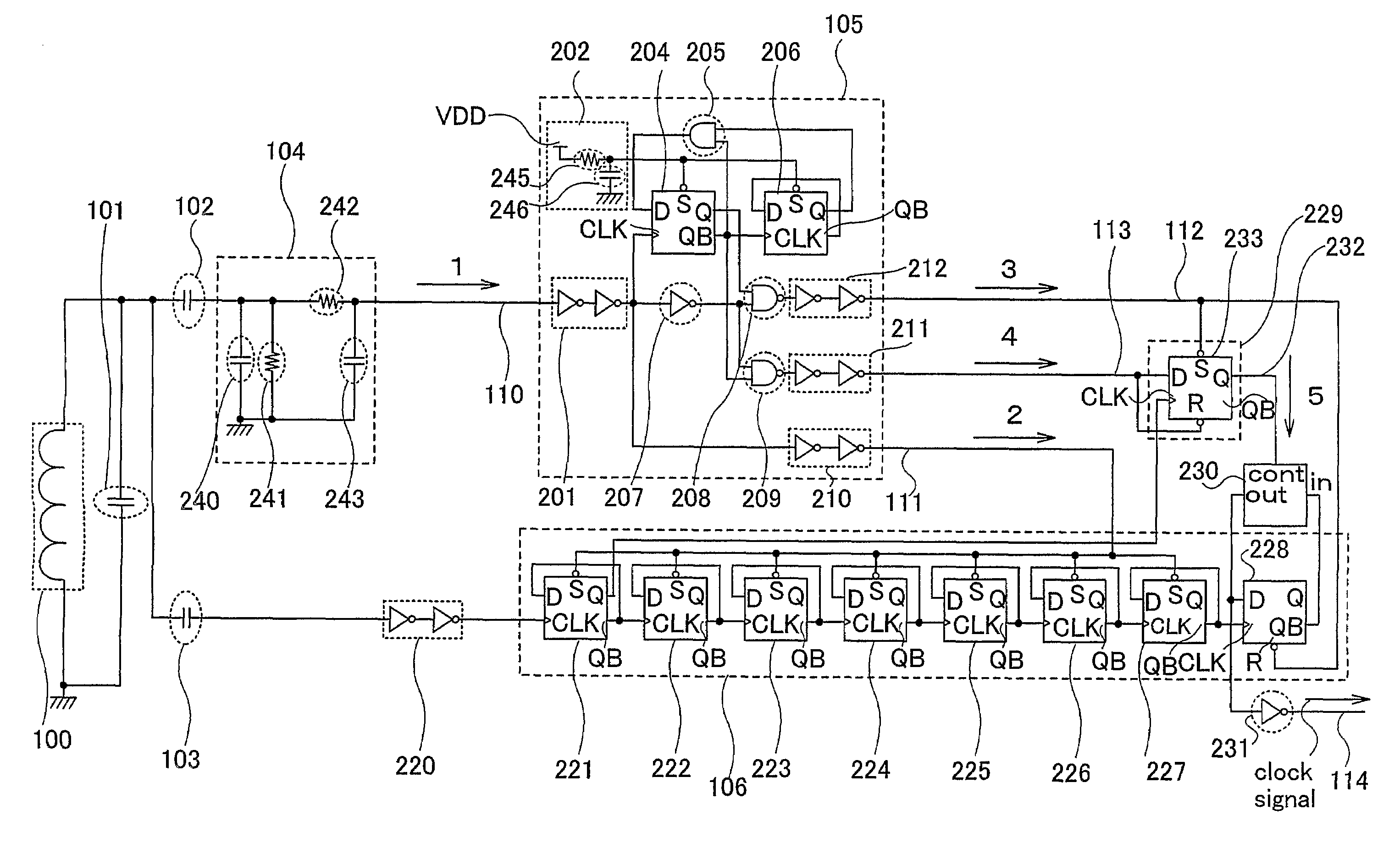
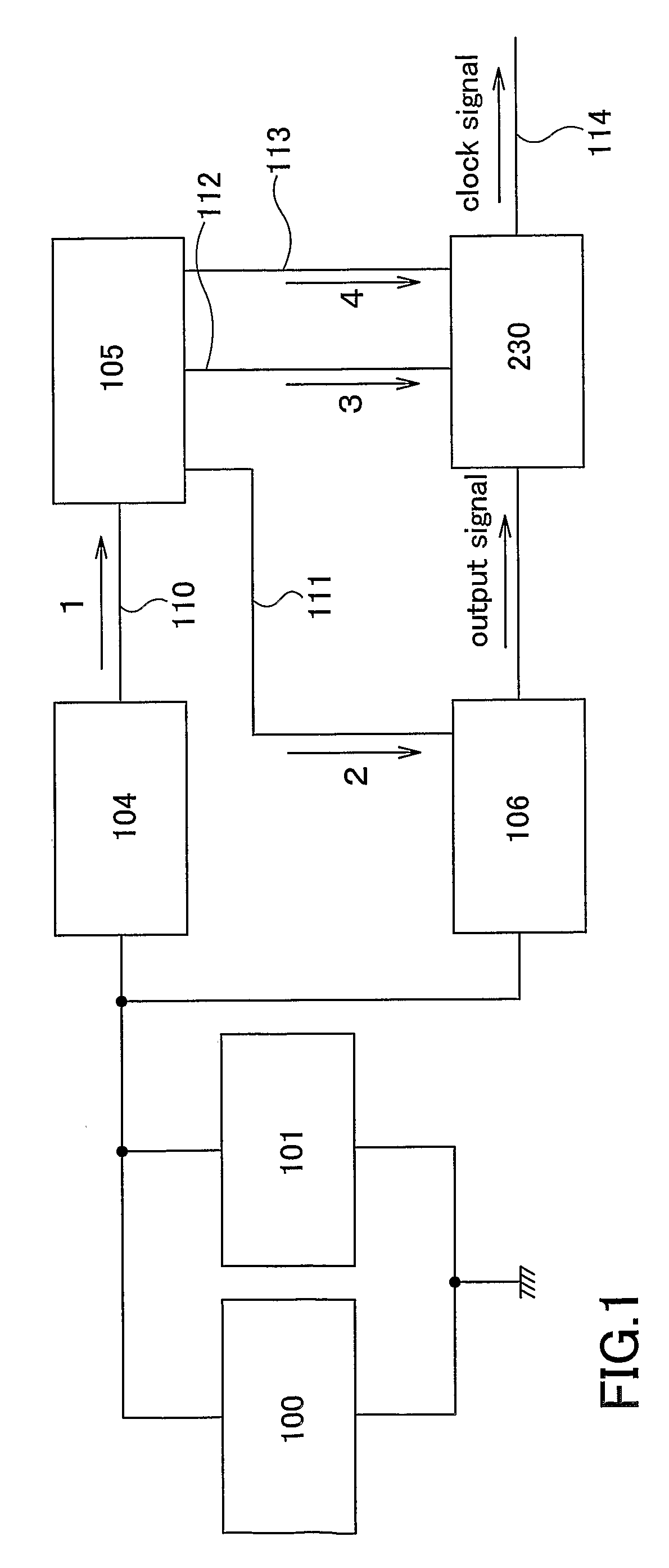
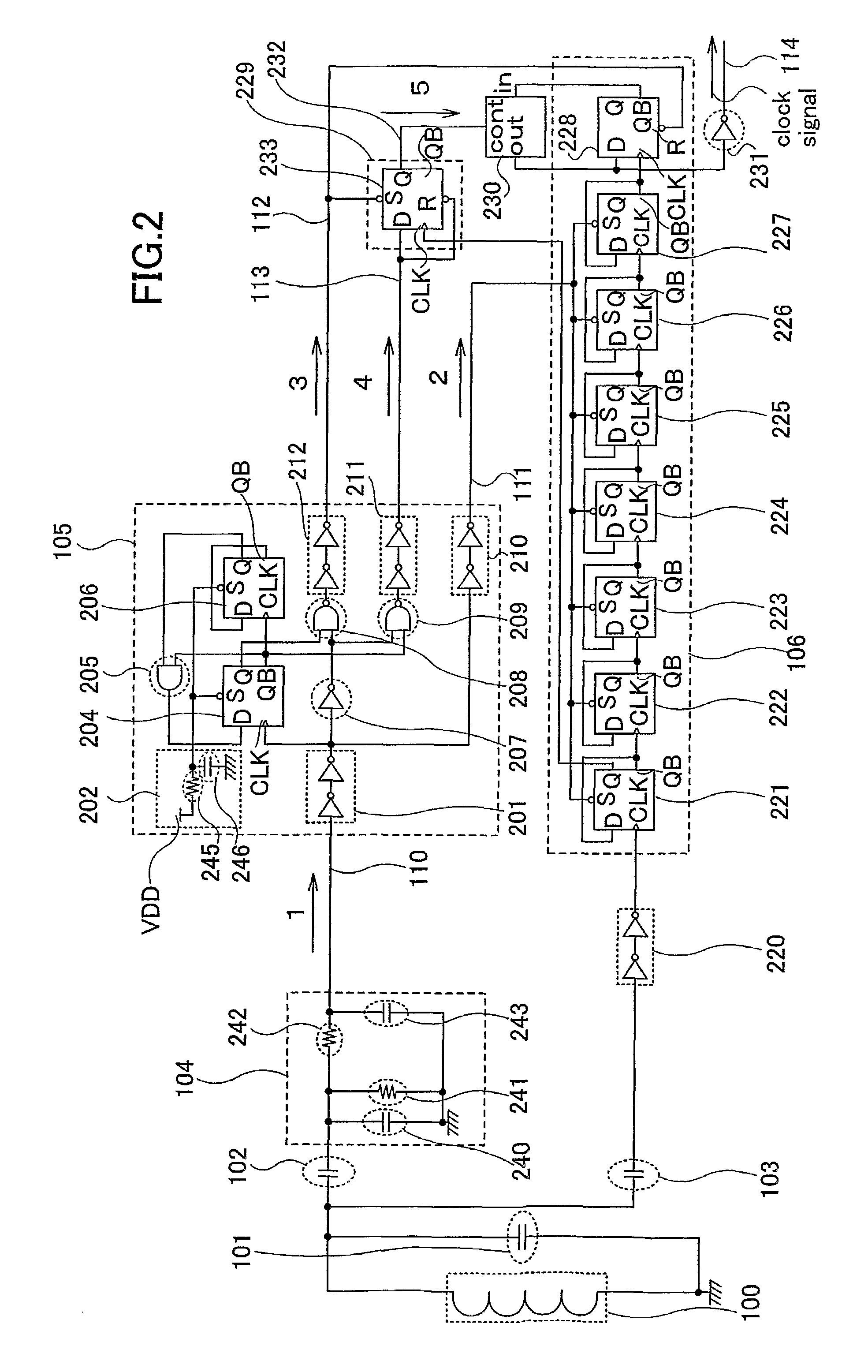
[0040]A configuration of a semiconductor device and operation thereof are described with reference to FIG. 2 and FIGS. 3A and 3B. The semiconductor device has the antenna 100, the resonant capacitor 101, capacitors 102 and 103, the demodulation circuit 104, the demodulated signal separation circuit 105, the divider circuit 106, a demodulated signal generating circuit 229, the correction circuit 230, a buffer circuit 220, and an inverter 231 (see FIG. 2).

[0041]The antenna 100 and the resonant capacitor 101 receive a carrier transmitted from a reader / writer. The received carrier is inputted to the demodulation circuit 104 and the divider circuit 106 through the capacitors 102 and 103 and the buffer circuit 220. The carrier has a waveform with a short pulse width (see the waveform of “carrier” of FIGS. 3A and 3B). FIG. 3B is an enlarged view of a dotted line portion 405 of FIG. 3A.

[0042]The demodulation circuit 104 generates the demodulated signal 1 from a carrier including 100% modula...

embodiment mode 2

[0057]In this embodiment mode, a configuration example of the correction circuit 230 in the divider circuit 106 is specifically described with reference to FIGS. 4A and 4B.

[0058]The correction circuit 230 has the input terminal in, the input terminal cont, and the output terminal out, as well as inverters 300 and 301 and NAND circuits 302 to 304 (see FIG. 4A). The NAND circuit 302 outputs the NAND logic of signals inputted from the input terminal in and the input terminal cont. The NAND circuit 303 outputs the NAND logic of signals that are obtained by inverting the signals inputted from the input terminal in and the input terminal cont by the inverters 300 and 301, respectively. The NAND circuit 304 outputs the NAND logic of output signals from the NAND circuits 302 and 303. An output signal from the NAND circuit 304 is outputted from the output terminal out.

[0059]The correction circuit 230 outputs the same signal as an input signal (denoted by “in” in the drawing) from the output ...

embodiment 1

[0061]Simulation results of clock signal generation by the semiconductor device of the invention are described with reference to FIGS. 5 and 6, which show the waveform of each signal. FIG. 6 is an enlarged view of a dotted line portion 150 of FIG. 5.

[0062]In FIG. 5, “carrier” shows the waveform of a carrier transmitted from a reader / writer, and “demodulated signal 1” shows the waveform of a signal obtained by demodulating the carrier. “Eighth stage CLK” shows the waveform of a signal that is obtained by dividing the carrier by the flip flops 221 to 227 and inputted to the CLK terminal of the eighth stage flip flop 228. “Eighth stage QB” shows the waveform of a signal outputted from the output terminal QB of the eighth stage flip flop 228. “Demodulated signal 5” shows the waveform of a signal obtained by separating pulses other than the first pulse from the demodulated signal 1. “Clock signal” shows the waveform of a clock signal outputted from the divider circuit.

[0063]When the carr...


PUM


Abstract

The invention provides a semiconductor device that generates a clock signal with a fixed pulse width from a carrier. The invention also provides a semiconductor device where data can be obtained accurately from a carrier using a clock signal with a fixed pulse width. Further, the invention provides a semiconductor device that has a simpler circuit configuration and a smaller scale, and consumes less power as compared to the PLL circuit. According to the invention, a signal obtained by dividing a carrier including 100% modulation is not used as a clock signal, and a correction circuit is used to generate a clock signal using a demodulated signal and a signal obtained by dividing the carrier including 100% modulation. According to the invention having such a configuration, a clock signal with a fixed pulse width can be generated.

Description

TECHNICAL FIELD[0001]The present invention relates to a semiconductor device that generates a clock signal from a carrier, and to a semiconductor device that operates using a clock signal generated from a carrier and communicates data wirelessly. Further, the invention relates to a semiconductor device that generates a clock signal from a carrier when using a communication system defined by ISO / IEC 15693 (JIS6323) or the like, which is the standard for vicinity wireless IC cards.BACKGROUND ART[0002]In a semiconductor device communicating data wirelessly, high frequency electromagnetic waves transmitted from a reader / writer are received by an antenna to generate a power supply needed for circuit operation. In addition, data is transmitted by affecting electromagnetic waves in some way by a signal and modifying the amplitude, frequency, phase (also called position) and the like of the electromagnetic waves. Such a change in the amplitude and the like of the electromagnetic waves is ca...

Claims


Application Information

Patent Timeline
Patent Type & Authority Patents(United States)
IPC IPC(8): H03D1/18
CPCH04L7/0331G06K19/0723H04L25/49
Inventor ATSUMI, TOMOAKI
Owner SEMICON ENERGY LAB CO LTD
Why Eureka
Try Eureka