

Nanoscale self-assembled organic dielectrics for electronic devices
- Summary
- Abstract
- Description
- Claims
- Application Information
AI Technical Summary
Benefits of technology
Problems solved by technology
Method used
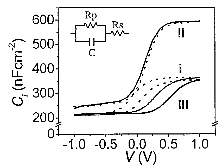
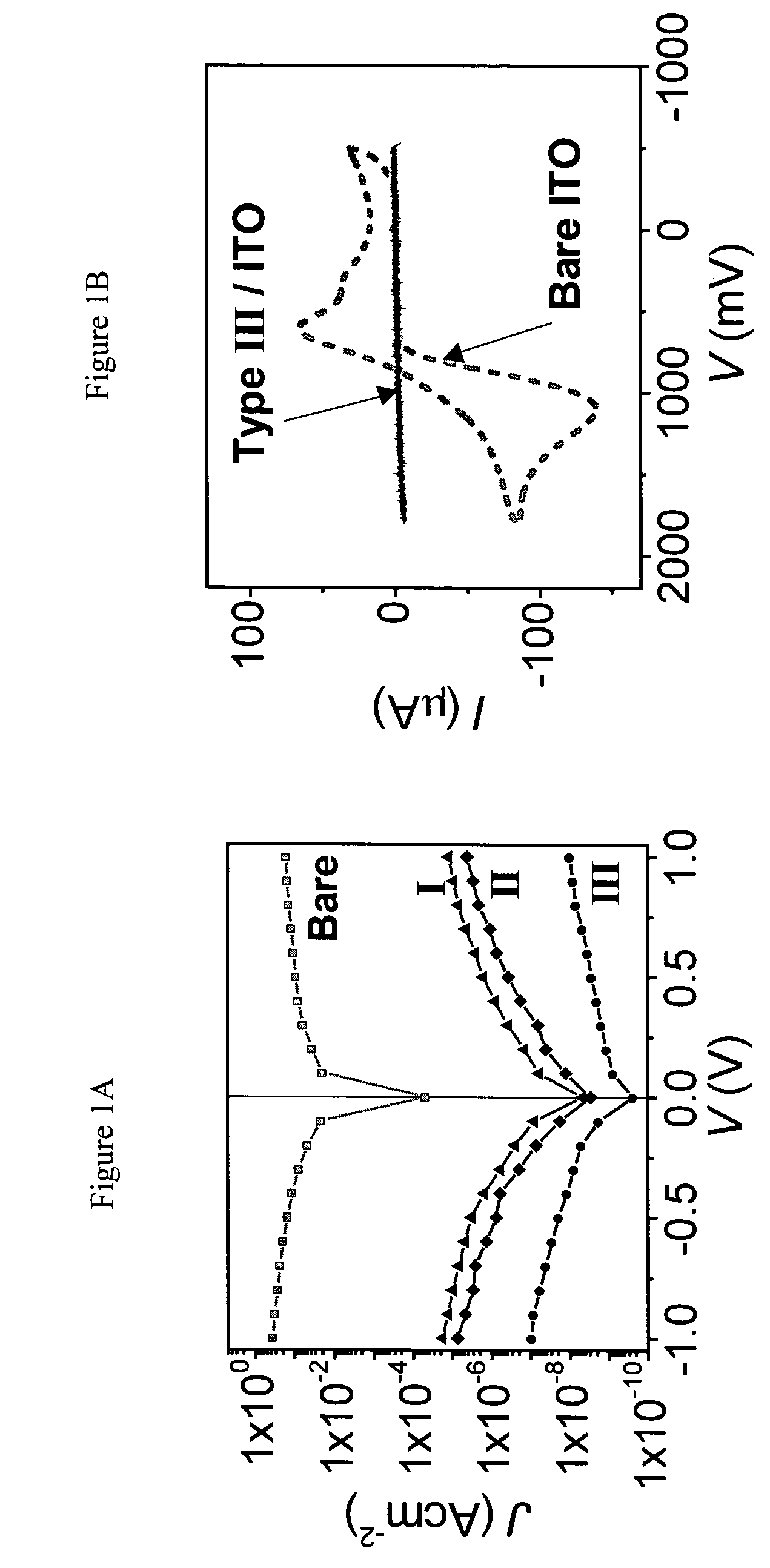
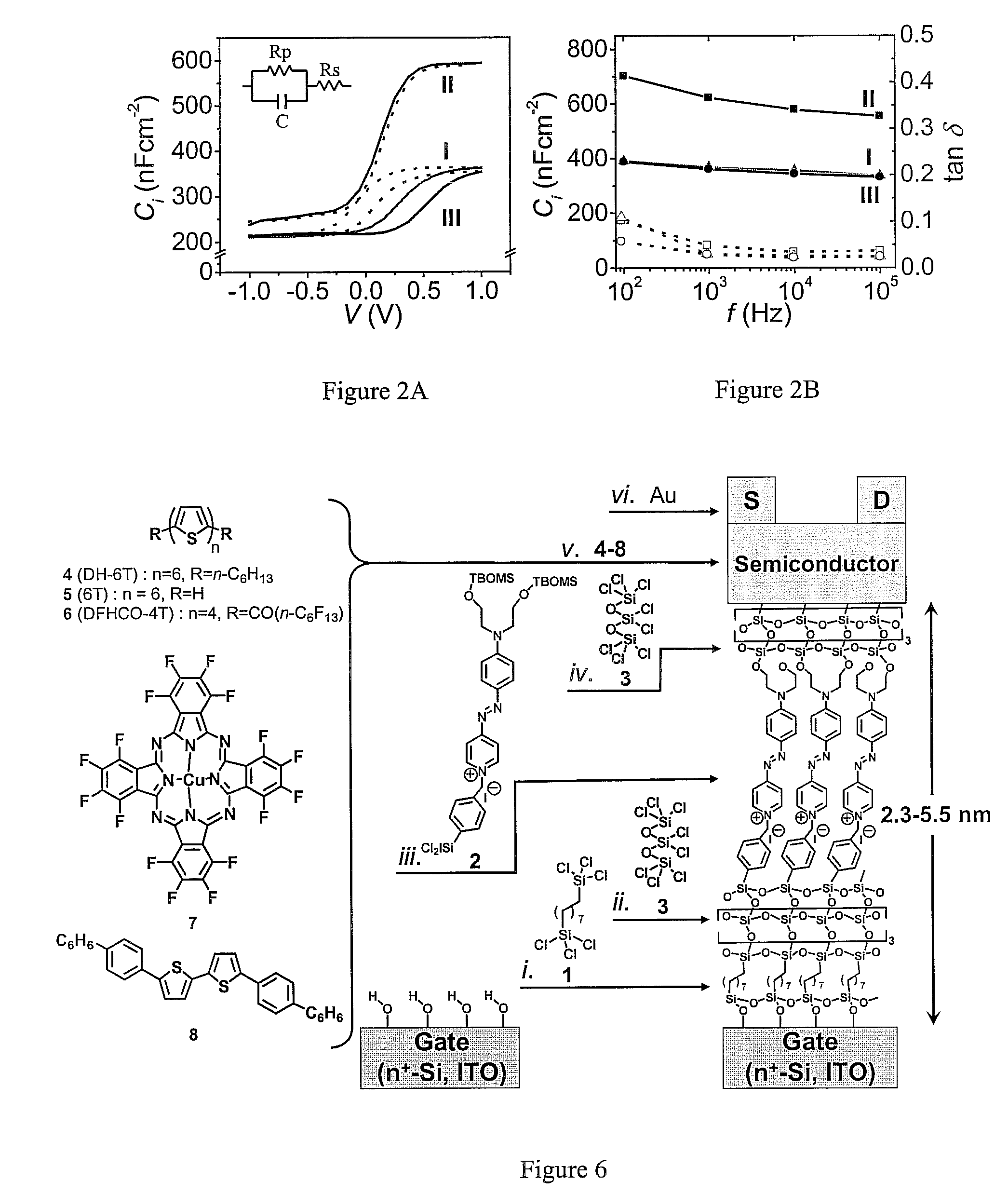
Image

Examples
example 1
[0040]The bis-trichlorosilane-functionalized alkyl chain (Cl3Si(CH2)8SiCl3) and octachlorotrisiloxane reagents were purchased from Gelest, and the stilbazonium salt precursor was prepared according to the aforementioned, incorporated patents and a literature procedure. See, also Zhu, P.; vad der Boom, M. E.; Kang, H.; Evmenenko, G.; Dutta, P.; Marks, T. J. Chem. Mater. 2002, 14, 4982 which is incorporated herein by reference in its entirety. Native oxide coated highly n-doped silicon (100) wafers were purchased from Montco Silicon Tech, Spring City, Pa. ITO-coated glass substrates (20Ω / sq; 20-30-Å rms roughness) were purchased from Donnelly Corp. Semiconductor 4 was synthesized and purified by the literature procedure, (Garnier, F.; Yassar, A.; Hajlaoui, R.; Horowitz, G.; Deloffre, F.; Servet, B.; Ries, S.; Alnot, P. J. Am. Chem. Soc. 1993, 115, 8716 (2002), incorporated herein by reference), and new compound 6 was synthesized and characterized by a straightforward methodology. See,...
example 2
[0042]Self-assembly procedure. All silicon wafers were cleaned with RCA solution, milli-Q water, and Piranha solution according to standard procedures and were dried as quickly as possible. For alkyl chain self-assembly, clean, dry wafers were placed in a glass holder and immersed in 1-10 mM solutions of Cl3Si(CH2)8SiCl3 in distilled toluene for 1 h at 0° C. under nitrogen. They were then washed with dry toluene twice and then with acetone. For hydrolysis, coated wafers were then immersed in acetone / water (5:1) for 1 h, then rinsed with acetone and methanol and blown dry with a nitrogen stream. Stilbazonium salt and octachlorotrisiloxane capping layers were deposited by procedures described in the literature, (see, Marks, J. Chem. Mater., 2002) and in the aforementioned incorporated patents.
example 3
[0043]Device fabrication. For TFTs, semiconducting materials (4-7) were vacuum deposited at 2-3×10⁶ Torr (500 Å, 0.2 Å / s) while maintaining the substrate temperature at 60° C. Gold electrodes were then vacuum deposited through shadow masks at 5-6×10⁻⁶ Torr (500 Å, 0.5 Å / s). For gold electrodes in MIS structures, the same procedure was employed.
PUM
 Abstract
Description
Claims
Application Information