Circuit board structure and manufacturing method thereof

a technology of circuit board and manufacturing method, which is applied in the direction of superimposed coating process, liquid/solution decomposition chemical coating, resistive material coating, etc., can solve the problems of failure, rough surface of led may be difficult to be processed or polished, and performance may be deteriorated, so as to enhance the effect of enhancing the insulating effect of the dielectric layer

Active Publication Date: 2010-03-04
IND TECH RES INST
View PDF20 Cites 6 Cited by
  • Summary
  • Abstract
  • Description
  • Claims
  • Application Information

AI Technical Summary

Benefits of technology

[0013]In the present invention, a metal buffer layer is first formed to cover a rough surface of the composite substrate, and then a surface of the metal buffer layer is polished to effectively enhance the insulating effect of the dielectric layer. Besides, a barrier layer is formed between the dielectric layer and the metal buffer layer to prevent metal atoms of the metal buffer layer from diffusing into the dielectric layer, thereby further enhancing the insulating effect of the dielectric layer.

Problems solved by technology

However, once the electric power and the working current are raised, the LED generates more heat and easily gets overheated, and thus, the performance of the LED may be deteriorated, and what's worse, a failure may occur.
However, such a composite substrate is extremely hard, so the rough surface thereof is difficult to be processed or polished.
Thus, compared with an ordinary metal circuit substrate, the composite substrate has a higher surface roughness, so that the insulating effect of the coated dielectric layer is weakened.
For example, in the circuit board structure provided by the ROC Patent M282455, the insulating effect of the dielectric layer is deteriorated due to the impact of diffusion effects of metal atoms or roughness of the metal composite substrate.
Moreover, in the heat sink provided by the ROC Patent I258333, the dielectric layer is mainly used for enhancing the heat dissipation effect, and no solutions about improving the insulating effect are proposed.

Method used


Image

  • Circuit board structure and manufacturing method thereof
  • Circuit board structure and manufacturing method thereof
  • Circuit board structure and manufacturing method thereof

Examples


Embodiment Construction

[0019]Reference will now be made in detail to the present embodiments of the invention, examples of which are illustrated in the accompanying drawings. Wherever possible, the same reference numbers are used in the drawings and the description to refer to the same or like parts.

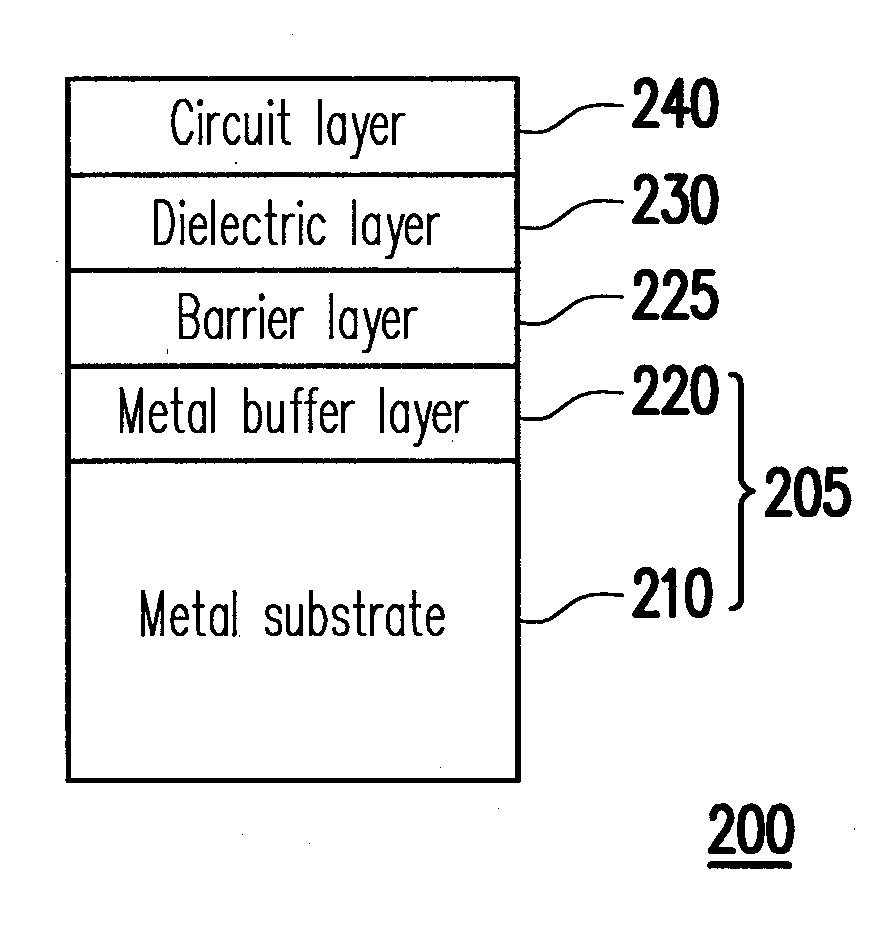
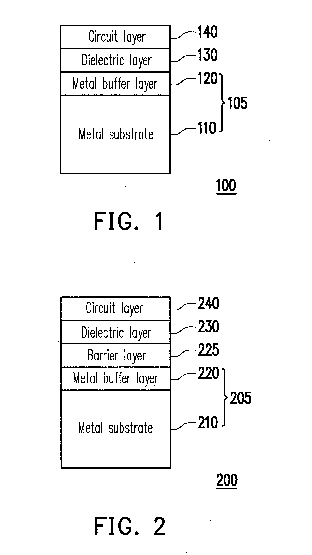
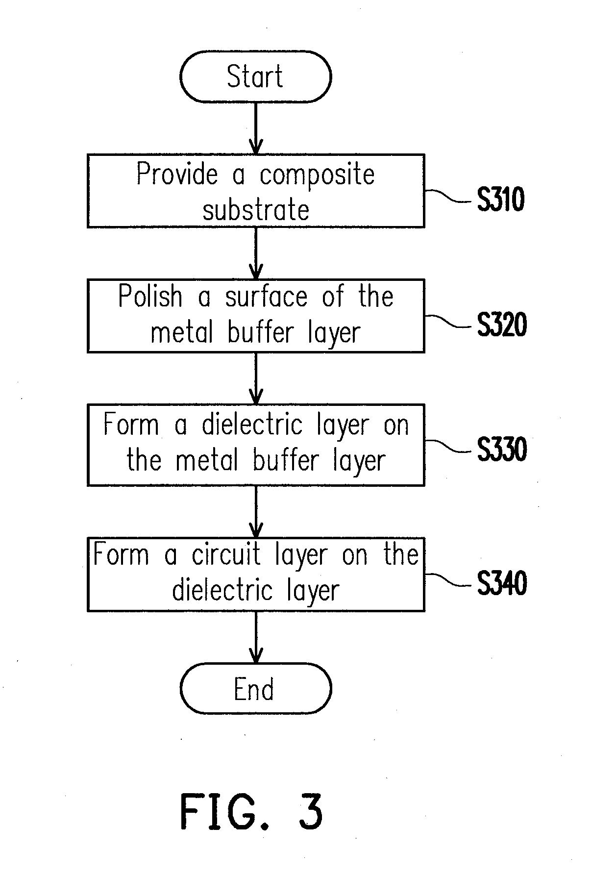
[0020]FIG. 1 shows a circuit board structure according to a first embodiment of the present invention. Referring to FIG. 1, a circuit board structure 100 includes a composite substrate 105, a dielectric layer 130, and a circuit layer 140. The composite substrate 105 includes a metal substrate 110 doped with non-metal powders and a metal buffer layer 120. The dielectric layer 130 is formed on an upper surface of the metal -buffer layer 120, and a surface of the metal buffer layer 120 facing the dielectric layer 130 is treated with a polishing process. The circuit layer 140 is formed on an upper surface of the dielectric layer 130. That is to say, the metal substrate 110, the metal buffer layer 120, the dielectr...


PUM

PropertyMeasurementUnit
thicknessaaaaaaaaaa
thicknessaaaaaaaaaa
thicknessaaaaaaaaaa

Abstract

A circuit board structure and a manufacturing method thereof are provided. The circuit board structure includes a composite substrate, a dielectric layer, and a circuit layer. The composite substrate includes a metal substrate doped with non-metal powders and a metal buffer layer. A surface of the metal buffer layer opposite to the other surface of the metal buffer layer in contact with the metal substrate is treated by a polishing process. The dielectric layer is formed on the polished surface of the metal buffer layer, and the circuit layer is formed on the dielectric layer. Alternatively, a barrier layer is interposed between the dielectric layer and the metal buffer layer for preventing a diffusion effect of the metal buffer layer.

Description

CROSS-REFERENCE TO RELATED APPLICATION[0001]This application claims the priority benefit of Taiwan application serial no. 97133281, filed on Aug. 29, 2008. The entirety of the above-mentioned patent application is hereby incorporated by reference herein and made a part of specification.BACKGROUND OF THE INVENTION[0002]1. Field of the Invention[0003]The present invention generally relates to a circuit board structure, in particular, to a circuit board structure with heat dissipation effect.[0004]2. Description of Related Art[0005]Recently, with the rapid development of technology, it has an increasingly high requirement on the heat dissipation effect of metal circuit boards of electronic devices. Taking a light emitting diode (LED) for example, the illuminating efficiency of the LED has been gradually enhanced after continuous research and improvement, such that its luminance is further raised to meet more demands from various products. In other words, in order to enhance the luminan...

Claims


Application Information

Patent Timeline
Patent Type & Authority Applications(United States)
IPC IPC(8): H05K1/03B05D5/12H05K1/02H05K1/00
CPCB82Y10/00H05K1/053H05K2201/0179H05K2203/025H05K2201/0251H05K2201/026H05K2201/0323H05K2201/0209
Inventor TAIN, RA-MINDAI, MING-JI
Owner IND TECH RES INST
Why Eureka
Try Eureka