Write and read assist circuit for SRAM with power recycling

a technology of assist circuit and sram, applied in the field of sram, can solve the problems of degrading vtrip, increasing the difficulty of achieving stable sram performance, and affecting the stability of snm,

Active Publication Date: 2010-03-16
ORACLE INT CORP
View PDF2 Cites 77 Cited by
  • Summary
  • Abstract
  • Description
  • Claims
  • Application Information

AI Technical Summary

Problems solved by technology

Historically, as circuit feature sizes are reduced and supply voltages are lowered, it has become increasingly difficult to achieve stable SRAM performance and design an SRAM cell that has both adequate static noise margin (SNM) and adequate trip voltage (Vtrip).
For SRAM cells in general, SNM and Vtrip are interdependent and design techniques that improve SNM, tend to degrade Vtrip and vice-versa.
Also, if the load is too weak relative to the drive transistor, SNM is degraded.
Due to the interdependent nature of the tradeoffs between write and read operations, it has become very difficult to achieve a SRAM design with high SNM and Vtrip.
Thus, SRAM design has become a delicate balance of the relative strengths of the passgate, drive, and load transistors.

Method used


Image

  • Write and read assist circuit for SRAM with power recycling
  • Write and read assist circuit for SRAM with power recycling
  • Write and read assist circuit for SRAM with power recycling

Examples


Embodiment Construction

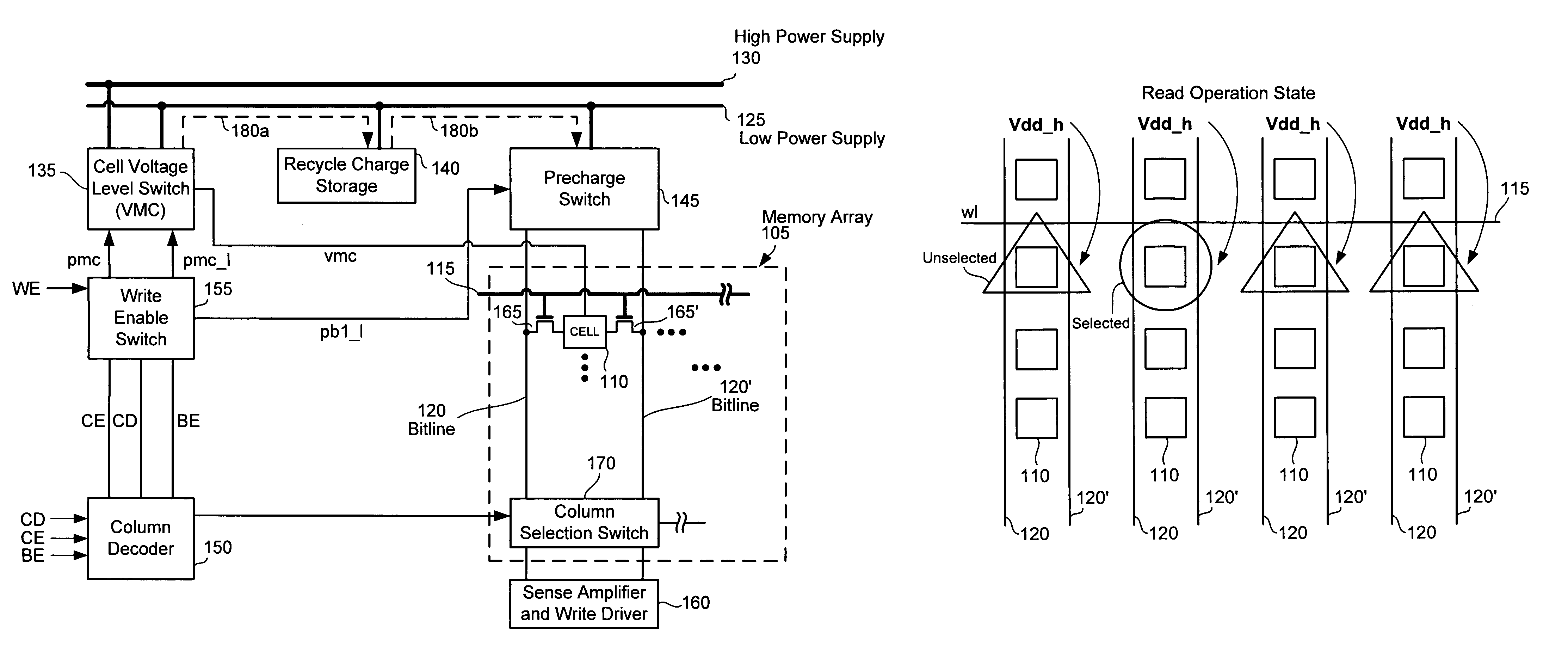
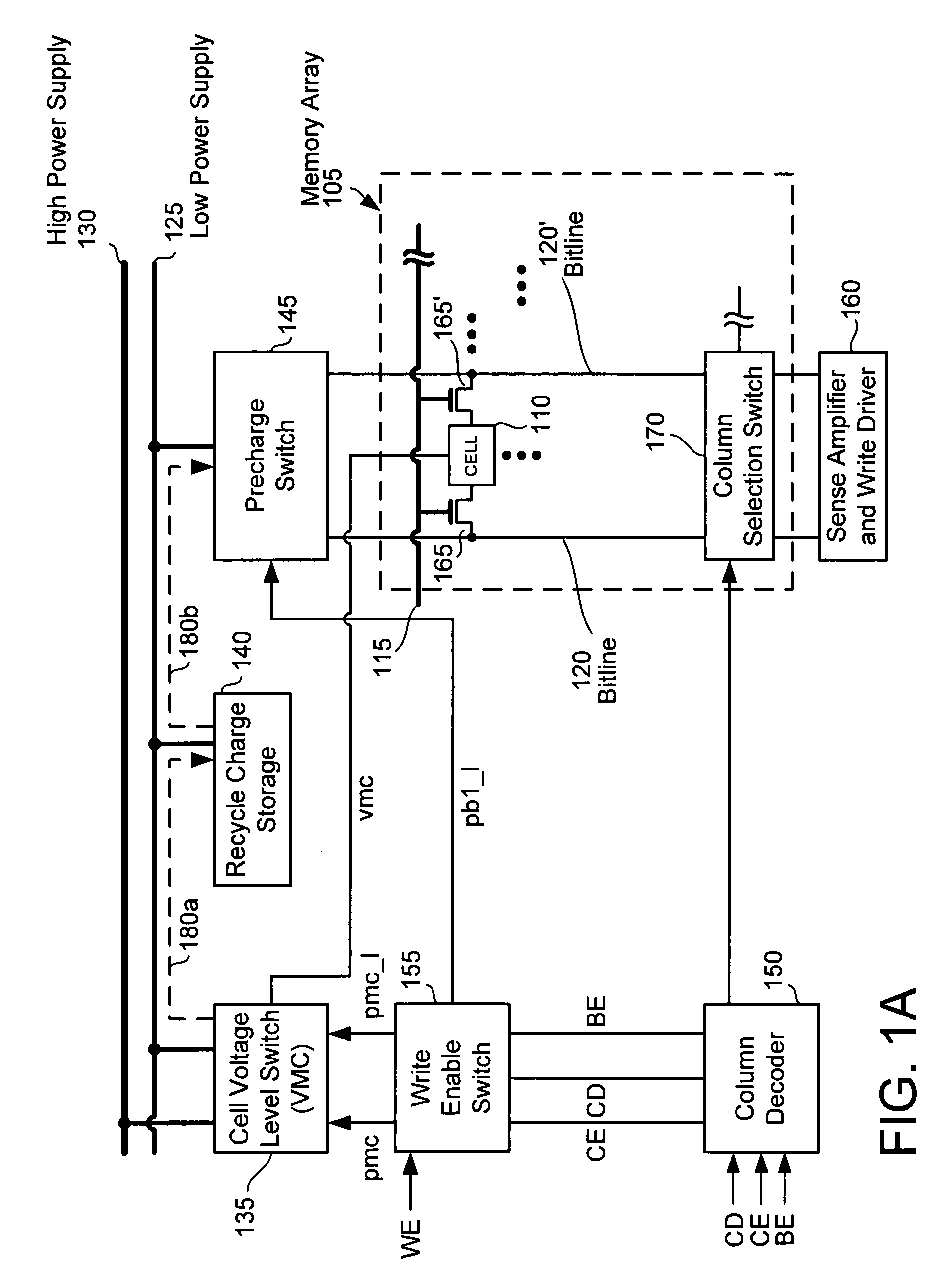
[0022]The following embodiments describe an apparatus and method for reading and writing data into a memory array and using charge recycling. It will be obvious, however, to one skilled in the art, that the present invention may be practiced without some or all of these specific details. In other instances, well known process operations have not been described in detail in order not to unnecessarily obscure the present invention.

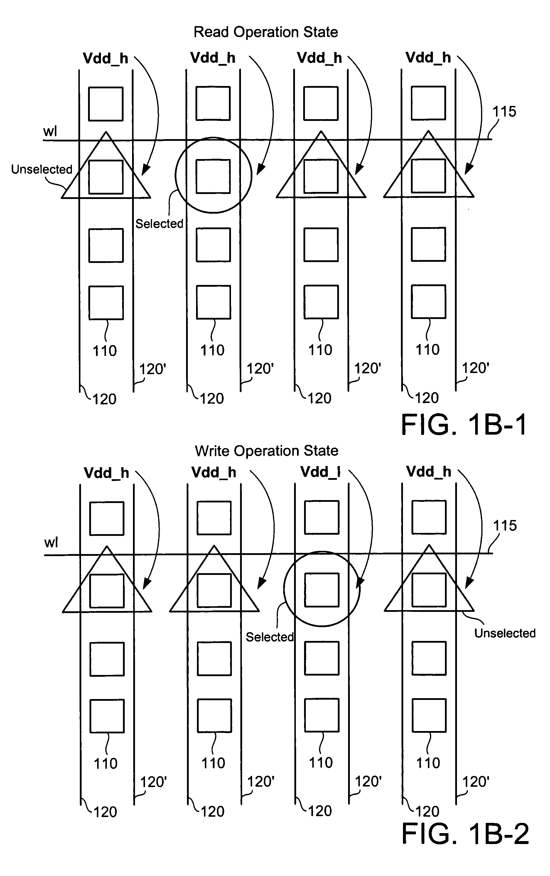
[0023]One design technique to improve the Vtrip margin during the write operation is reducing the power supply voltage to the SRAM cells 110, but lowering the SRAM power supply voltage also reduces the SRAM SNM margin. Conversely, increasing the power supply voltage to the SRAM cells 110 improves the SNM margin, which is important for the read operation. Implementation of the claimed design technique uses two power supply voltages 125 and 130, selectively applied to the SRAM cells 110 during read and write operations. Switches are used to control which power...


PUM


Abstract

A memory circuit for reading and writing data into a SRAM memory array using charge recycling is presented. The write and read circuit includes a cell voltage level switch, a recycle charge storage, a precharge switch, a write enable switch, and column decoder. The cell voltage level switch is connected to a low power supply and a high power supply and has two states of operation: a write operation state and a read operation state. For each state of operation, the voltage level switch selectively provides a power supply if a column has been selected or if the operation is a read or write. The recycle charge storage stores excess charge from SRAM cells after a read operation or after a write operation in unselected columns. After the read or write operation, the recycle charge storage discharges excess charge to the bitlines during bitline precharging.

Description

BACKGROUND OF THE INVENTION[0001]1. Field of the Invention[0002]The present invention relates generally to semiconductor memory devices and more particularly to an improved SRAM design for more stable SRAM performance and reduced power consumption.[0003]2. Description of the Related Art[0004]Historically, as circuit feature sizes are reduced and supply voltages are lowered, it has become increasingly difficult to achieve stable SRAM performance and design an SRAM cell that has both adequate static noise margin (SNM) and adequate trip voltage (Vtrip). The trip voltage (Vtrip) is a measure of the ability of a cell to write digital data into a SRAM cell.[0005]The SNM quantifies the amount of voltage noise required at the internal nodes of the SRAM cell to flip the state of the digital data stored in the SRAM cell. The SNM may be determined graphically by plotting the voltage transfer curve of one of the inverters that comprises the latch of the SRAM cell and inverting the transfer curv...

Claims


Application Information

Patent Timeline
Patent Type & Authority Patents(United States)
IPC IPC(8): G11C11/00
CPCG11C5/147G11C11/417G11C11/419
Inventor PARK, HEECHOULKIM, SONGKWONG, LANCELOT
Owner ORACLE INT CORP
Why Eureka
Try Eureka