Light emitting device having pixel portion surrounded by first sealing material and covered with second sealing material
Inactive Publication Date: 2010-04-20
SEMICON ENERGY LAB CO LTD
View PDF76 Cites 40 Cited by
Summary
Abstract
Description
Claims
Application Information
AI Technical Summary
This helps you quickly interpret patents by identifying the three key elements:
Problems solved by technology
Method used
Benefits of technology
Benefits of technology
[0018]The present invention has a top surface emission structure in which a substrate, with light emitting elements formed thereupon, is bonded to a transparent sealing substrate. A pixel region is covered over its entire surface by a transparent second sealing material when bonding the two substrates, and is surrounded by a first sealing material (having a higher viscosity than the second sealing material) that contains a gap material (filler, fine particles, or the like) for maintaining a gap between the two substrates. The first sealing material and the second sealing material thus seal the light emitting element.
[0020]Therefore, in the present invention, a pattern shape of the first sealing material is formed into a pattern having no bent portion (line shape) without making the pattern shape into the square shape, the inverted “c” shape or the “U” shape. Opening portions (four locations) are formed in the corners, which allow air bubbles to escape therethrough. By forming the opening portions, the low viscosity second sealing material is pushed out in the direction of the opening portion of the corners when bonding the two substrates using the low viscosity second sealing material. The two substrates can thus be sealed without air bubbles mixing in on the pixel region. In addition, a pattern for the high viscosity first sealing material may be slightly curved so that air bubbles do not form. Further, it is preferable that the substrate surfaces on the sealing side be smooth and have superior levelness so that bubbles do not mix in.
[0021]Further, there are cases in which a circumferential portion of the second sealing material will spread out from the opening portions (four locations), forming a bulging out shape (protruding shape), depending upon the viscosity of the second sealing material and the manner in which it is pushed out. There are also cases in which the circumferential portion of the second sealing material will form a shape that enters into the inside of the opening portions. Note that the adhesive strength between the two substrates can be increased in order to increase the contact adhesive surface area if there is provided a bulging out shape.
[0023]Further, a location of maximum load applied when a shock is received from the outside can be set to the location of the first sealing material (only the first sealing material has the gap material) disposed outside of the pixel region, and the load can be prevented from being applied to the pixel region. Further, this is a structure in which the first sealing materials are symmetrically disposed, and loads are applied uniformly and with a good balance. Shocks from the outside can therefore be uniformly diffused. Further, the first sealing materials have a symmetrical shape, and are disposed symmetrically, and therefore a very constant substrate gap can be maintained. That is, a light emitting device having an even more robust mechanical strength can be made by using the structure of the present invention.
Problems solved by technology
Since an EL material is deterioratable resulted from being oxidized or absorbed due to oxygen or moisture, there has been a problem that the luminous efficiency of a light emitting element is decreased or the lifetime thereof is shorted.
Thin substrates have a disadvantage, however, in that they are weak with respect to shocks.
Further, there is a fear in that the second electrode will react with the constituents contained in the sealing materials.
Method used
Image
Click on the blue label to locate the original text in one second.
Reading with bidirectional positioning of images and text.
Examples
embodiment mode 1
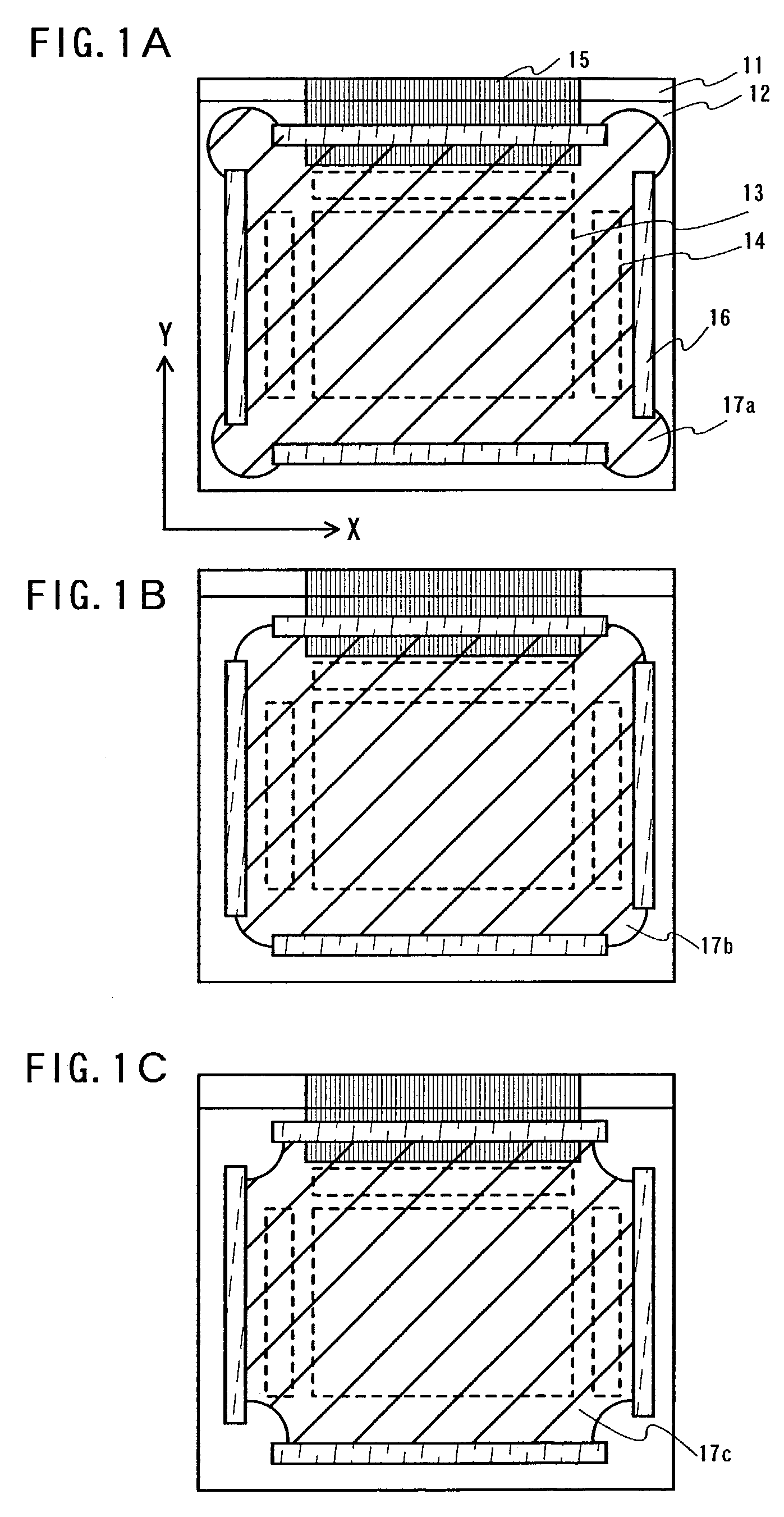
[0101]FIG. 1A is a top view of an active matrix light emitting device that implements the present invention.
[0102]In FIG. 1A, reference numeral 11 denotes a first substrate, reference numeral 12 denotes a second substrate, reference numeral 13 denotes a pixel portion, reference numeral 14 denotes a driver circuit portion, reference numeral 15 denotes a terminal portion, reference numeral 16 denotes first sealing materials, and reference numeral 17a denotes a second sealing material.
[0103]There are no specific limitations placed on the material used for the first substrate 11. It is preferable, however, to use substrates having identical thermal expansion coefficients for the first substrate 11 and the second substrate 12 because the two substrates are bonded together. A substrate having transparency, for example, a glass substrate, a quartz substrate, or a plastic substrate, is used for the first substrate 11 material if a bottom surface emission light emitting device is manufacture...
embodiment mode 2
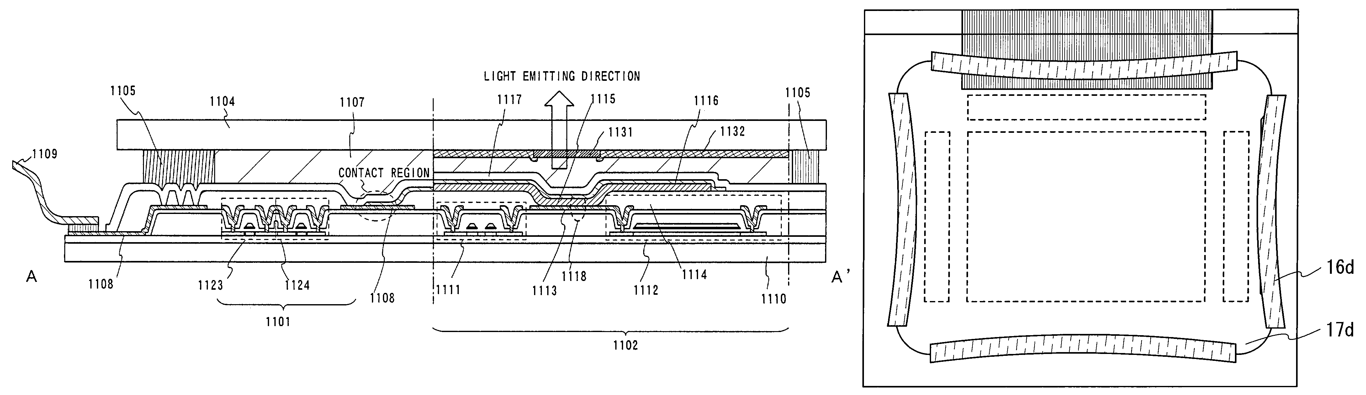
[0119]A portion of a cross sectional structure of a pixel portion of the present invention is shown here in FIG. 3A.
[0120]In FIG. 3A, reference numeral 300 denotes a first substrate, reference numerals 301a and 301b denote insulating layers, reference numeral 302 denotes a TFT, reference numeral 308 denotes a first electrode, and reference numeral 309 denotes an insulator. Reference numeral 310 denotes an EL layer, reference numeral 311 denotes a second electrode, reference numeral 312 denotes a transparent protective layer, reference numeral 313 denotes a second sealing material, and reference numeral 314 denotes a second substrate.
[0121]The TFT 302 (p-channel TFT) formed on the first substrate 300 is an element for controlling current flowing in the light emitting EL layer 310, and reference numeral 304 denotes a drain region (or a source region) thereof. Further, reference numeral 306 denotes a drain electrode (or a source electrode) that connects a first electrode and the drain ...
embodiment mode 3
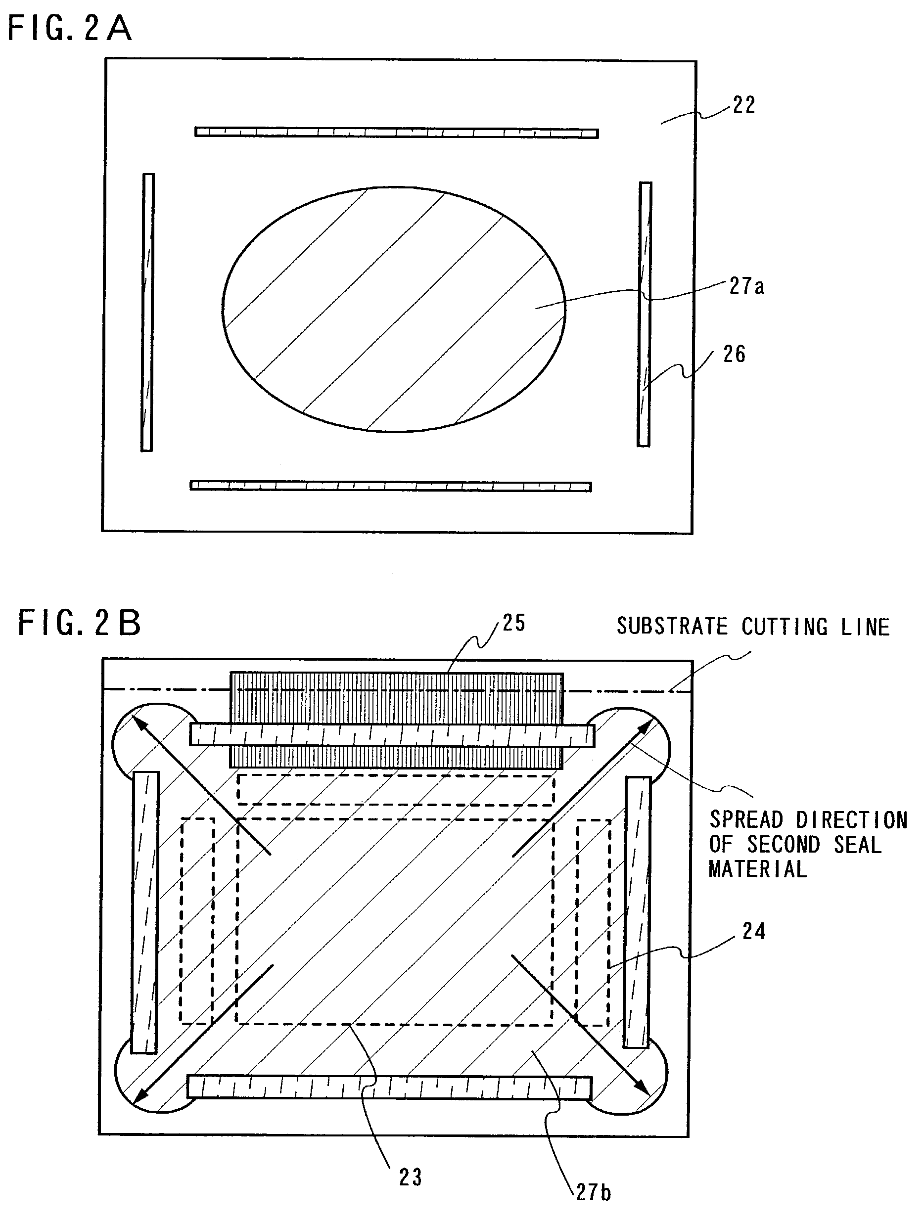
[0135]A case of forming a plurality of pixel portions on one substrate, that is, an example of multiple patterns, is shown in FIGS. 4A to 4E.
[0136]An example of forming four panels using one substrate is shown here.
[0137]First sealing materials 32 are formed first in a predetermined location on a second substrate 31 by using a dispenser apparatus under an inert gas atmosphere. (See FIG. 4A.) A material that contains a filler (diameter 6 μm to 24 μm) and having a viscosity of 370 Pa·s is used as a translucent sealing material for the first sealing materials 32. Further, data that shows the relationship between the size of the filler contained in the sealing material and the adhesive strength is shown in FIG. 9. Furthermore, the first sealing material 32 can be formed by print process because it has a simple sealing pattern. Next, a transparent second sealing material 33 is dripped on the region surrounded by the first sealing materials 32 (with openings in four corners) (see FIG. 4B)...
PUM
Abstract
A light emitting device having a structure in which oxygen and moisture are prevented from reaching light emitting elements, and a method of manufacturing the same, are provided. Further, the light emitting elements are sealed by using a small number of process steps, without enclosing a drying agent. The present invention has a top surface emission structure. A substrate on which the light emitting elements are formed is bonded to a transparent sealing substrate. The structure is one in which a transparent second sealing material covers the entire surface of a pixel region when bonding the two substrates, and a first sealing material (having a higher viscosity than the second sealing material), which contains a gap material (filler, fine particles, or the like) for protecting a gap between the two substrates, surrounds the pixel region. The two substrates are sealed by the first sealing material and the second sealing material. Further, reaction between electrodes of the light emitting elements (cathodes or anodes) and the sealing materials can be prevented by covering the electrodes with a transparent protective layer, for example, CaF2, MgF2, or BaF2.
Description
BACKGROUND OF THE INVENTION[0001]1. Field of the Invention[0002]The present invention relates to a semiconductor device having a circuit composed of a thin film transistor (hereinafter, TFT) and a method for manufacturing the semiconductor device. In particular, the present invention relates to an electronic device onboard an electric optical device typified by a liquid crystal display panel and a light emitting display device having an organic compound light emitting layer as components.[0003]A semiconductor device in this specification means comprehensive semiconductor devices such as an electric optical device, a semiconductor circuit, and an electronic device.[0004]2. Description of the Related Art[0005]In recent years, study of a light emitting device having an EL element as a self-luminous element has become vigorous. In particular, a light emitting device using an organic material as an EL material has attracted an attention. The light emitting device is also referred to as a...
Claims
Application Information
Patent Timeline
Application Date:The date an application was filed.
Publication Date:The date a patent or application was officially published.
First Publication Date:The earliest publication date of a patent with the same application number.
Issue Date:Publication date of the patent grant document.
PCT Entry Date:The Entry date of PCT National Phase.
Estimated Expiry Date:The statutory expiry date of a patent right according to the Patent Law, and it is the longest term of protection that the patent right can achieve without the termination of the patent right due to other reasons(Term extension factor has been taken into account ).
Invalid Date:Actual expiry date is based on effective date or publication date of legal transaction data of invalid patent.

