

Scan compression architecture for a design for testability compiler used in system-on-chip software design tools
a compiler and design technology, applied in the direction of electronic circuit testing, measurement devices, instruments, etc., can solve the problems of test cost in terms of test data volume and test time, and achieve the effect of reducing testing cos
- Summary
- Abstract
- Description
- Claims
- Application Information
AI Technical Summary
Benefits of technology
Problems solved by technology
Method used
Image

Examples
Embodiment Construction
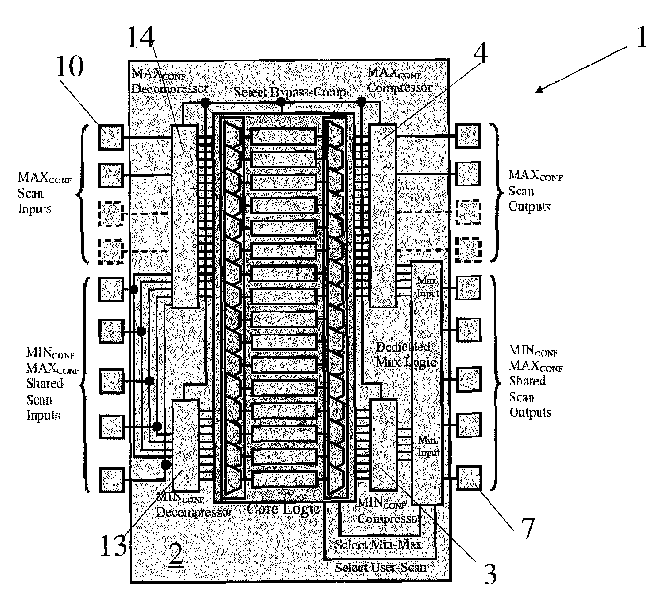
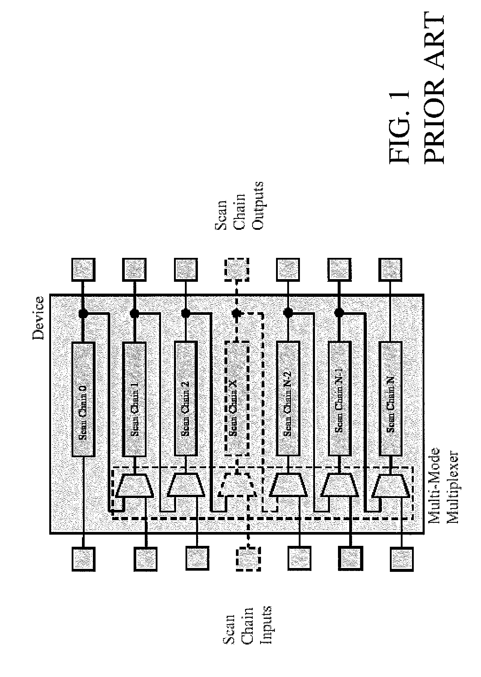
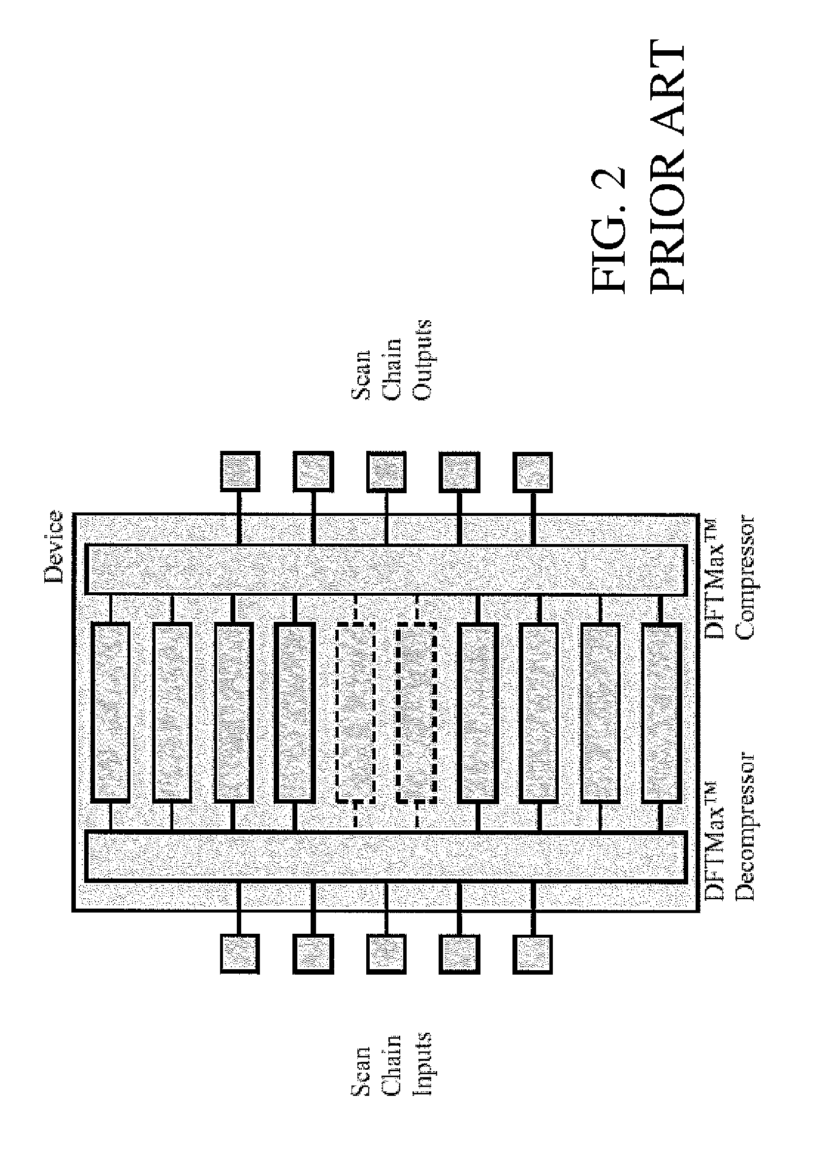
[0031]With reference to the figures, and in particular to the example shown in FIGS. 3 to 7, an improved scan compression architecture according to the present invention is represented by reference numeral 1. Reference numeral 1 corresponds to the architecture from its initial set up to its final layout through the design activity performed by a design for testability compiler.
[0032]This improved scan compression architecture 1 has been specifically designed for a design for a testability compiler incorporated into a standard software tool. More particularly, the improved scan compression architecture 1 is described with reference to a specific design for a testability compiler, and is included in a software standard tool known as Synopsys. This is only for illustration purposes and does not limit the scope of the present invention.
[0033]As will be apparent from the following description and claims, the improved scan compression architecture 1 may be realized through the design acti...
PUM
 Abstract
Description
Claims
Application Information