Deep trench isolation for power semiconductors

a technology of power semiconductors and trenches, applied in the direction of semiconductors, semiconductor devices, electrical apparatus, etc., can solve the problems of reducing the reliability of isolation structures, reducing the efficiency of isolation structures, and imposing barriers on junction isolation smart power technologies, so as to achieve the effect of reducing or avoiding breakdown at weaknesses in isolation structures, improving reliability and stability, and substantially improving reverse blocking voltage of structures

Active Publication Date: 2010-05-25
SEMICON COMPONENTS IND LLC
View PDF4 Cites 17 Cited by
  • Summary
  • Abstract
  • Description
  • Claims
  • Application Information

AI Technical Summary

Benefits of technology

[0015]By dividing the voltage, the reverse breakdown voltage characteristics such as voltage level, reliability and stability can be improved for a given area of device, or for a given complexity of device, and avalanche breakdown at weaknesses in isolation structures can be reduced or avoided. Alternatively, for a given level of reliability, the reverse blocking voltage of the structure can be substantially improved. The bias arrangement can be used to divide the voltage to obtain a maximum overall breakdown voltage.

Problems solved by technology

Junction Isolated smart power technologies have the drawback of large lateral isolation structures, the area consumed by such structures being dependent on the required blocking voltage.
However, SOI is still expensive.
Moreover, it has some inherent drawbacks for power switching and high voltage applications: (1) in order to reduce the effect of the back-gate effect (substrate potential), the buried oxide needs to be thick, (2) a thick oxide poses a barrier to the heat generated in a power switch due to the much lower thermal diffusivity in oxide compared to silicon.
Hence, the devices will be much more prone to thermal destruction upon power switching, and have to be designed accordingly.

Method used


Image

  • Deep trench isolation for power semiconductors
  • Deep trench isolation for power semiconductors
  • Deep trench isolation for power semiconductors

Examples


first embodiment

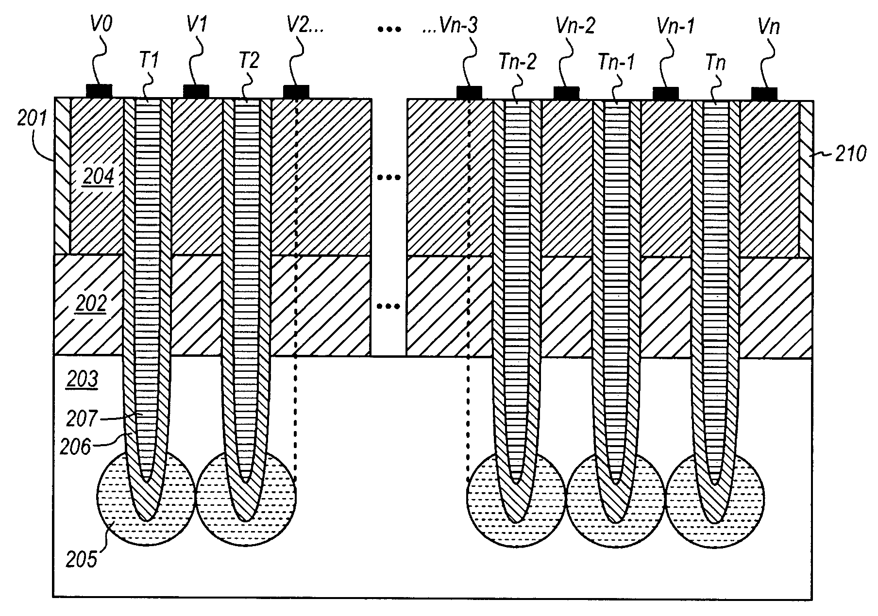
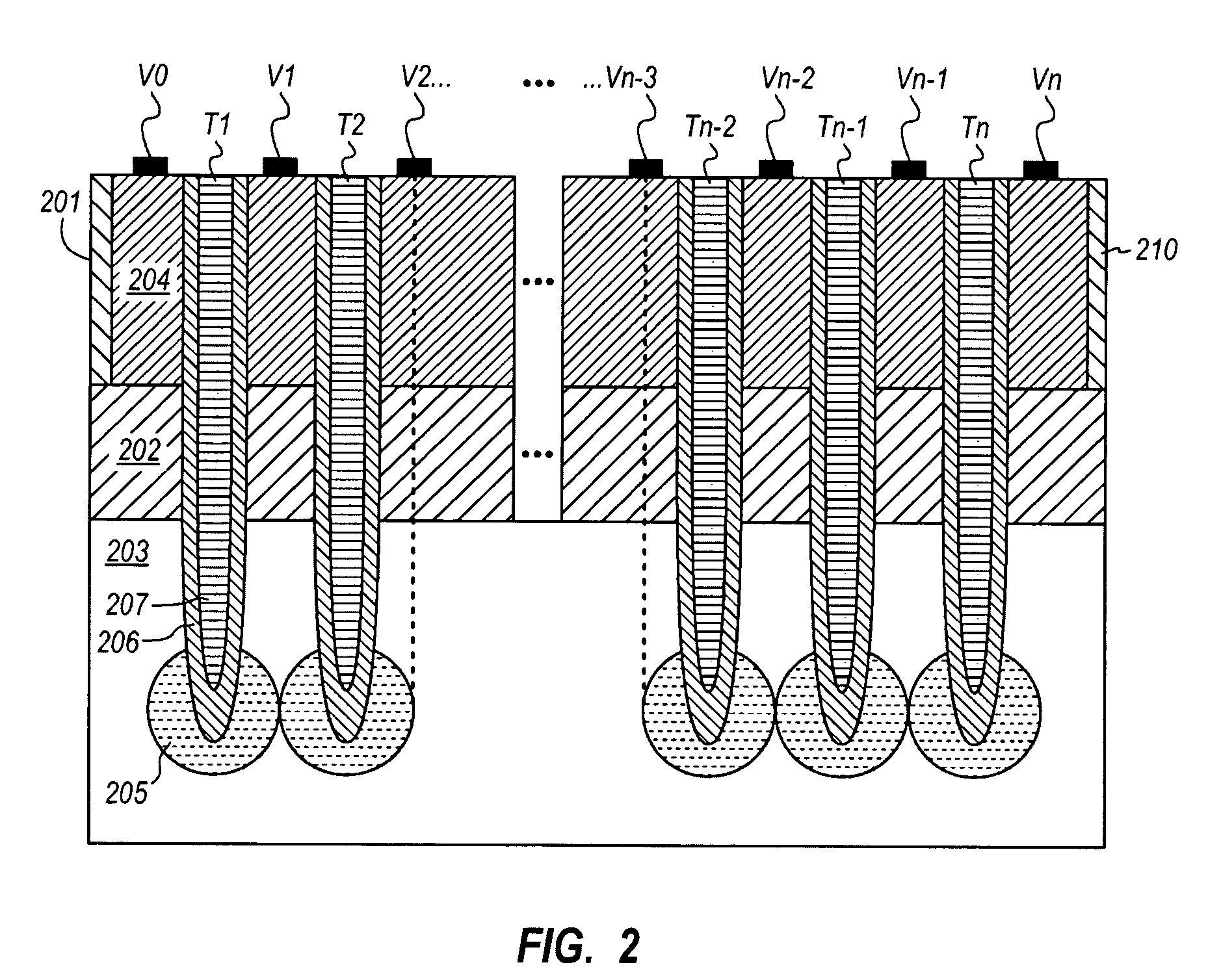
[0036]One semiconductor device (e.g. an active device such as a transistor) is located in the left-side epitaxial-pocket (201), and the adjacent semiconductor device (e.g. an active device such as a transistor) is located in the right-hand side epitaxial-pocket (210). In between them, a number (n) of trenches (Tn) are provided. Between each trench, a contacted semiconductor region, e.g. silicon region is present. The contact is biased to a given potential Vi (i=1, . . . n−1). Each trench is similar to the structure shown in FIG. 1. In this first embodiment, the polysilicon layer (207) is left floating. In general, the upper layer between two successive trenches is a highly doped region (204) having a typical doping level between 1018 and 1020 cm−3 and has the same conductivity type as that of a lower layer in the form of buried layer (202). While in this first preferred embodiment, the buried layer (202) is present and has a conductivity type opposite to the conductivity type of the...

second embodiment

[0037]In a second embodiment, the polysilicon layer (207) can be contacted and biased to an optimum potential. As many trenches as required can be put next to each other. In practice, four trenches are typically sufficient for maximum gain in reverse blocking voltage.

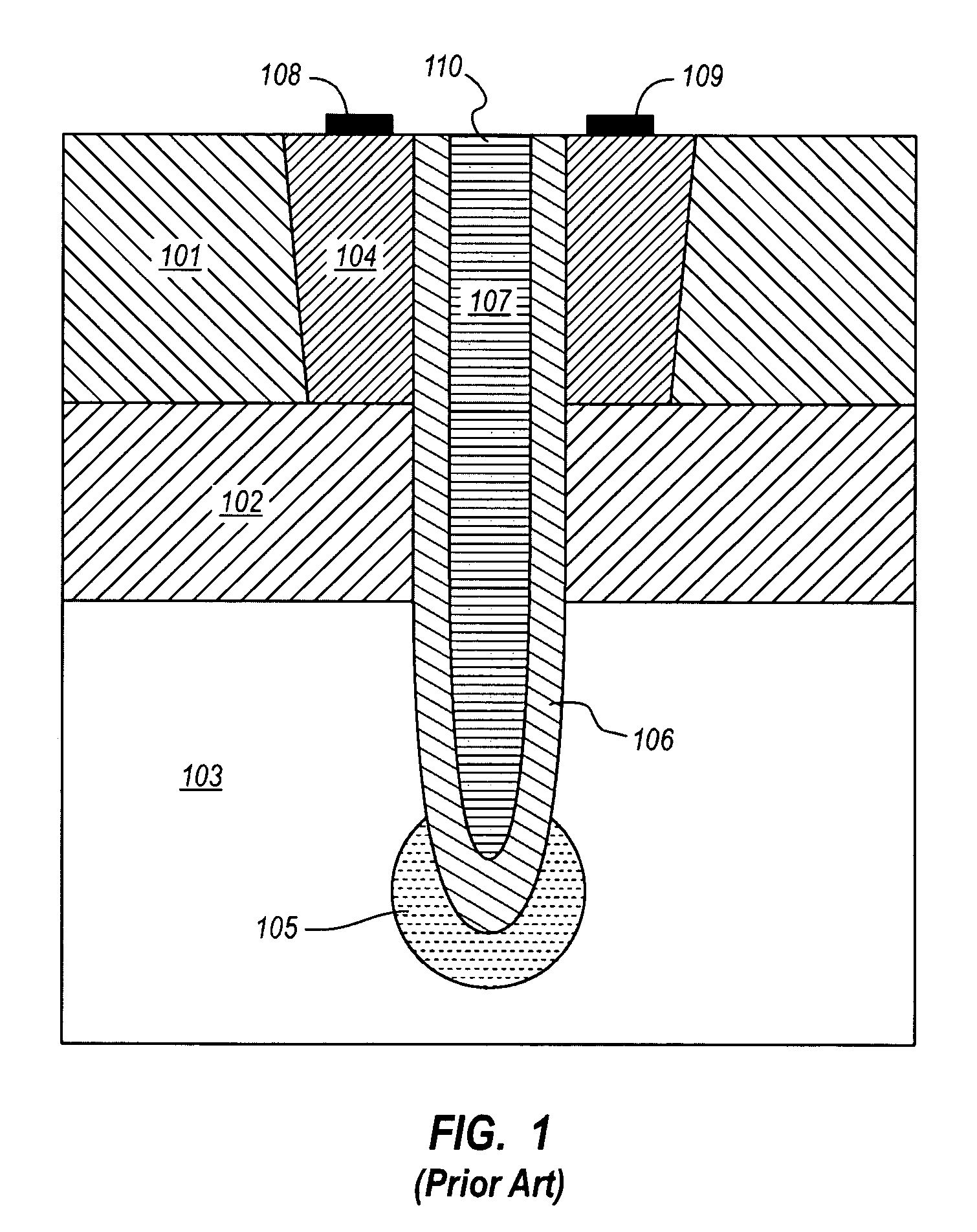
[0038]A simple analytical model for the single and double trench isolation structures, using a capacitive network will now be explained. The model is based on a capacitor divider network, which in general for a single trench (referring to FIG. 1):

[0039]Vpoly=CdrainCtot·Vdrain+CsourceCtot·Vsource+CsubsCtot·Vsubs(2)

in which:

Ctot=Csubs+Csource+Cdrain   (3)

“Source” refers to contact (108), “drain” refers to contact (109), “gate” refers to region (110), “subs” refers to the substrate (103).

[0040]The capacitance of the source, drain and substrate regions depends on the depth of the trench, the thickness of the epitaxial layer of the second conductivity type, e.g. the n-type epitaxial layer, and the out-diffusion of the BLN, t...


PUM


Abstract

An integrated power semiconductor device has an isolation structure having two or more isolation trenches, and one or more regions in between the isolation trenches, and a bias arrangement coupled to the regions to divide a voltage across the isolation structure between the isolation trenches. By dividing the voltage, the reverse breakdown voltage characteristics such as voltage level, reliability and stability can be improved for a given area of device, or for a given complexity of device, and avalanche breakdown at weaknesses in isolation structures can be reduced or avoided.

Description

CROSS-REFERENCE TO RELATED APPLICATIONS[0001]This patent application claims the benefit of European Patent Application Serial No. 07010439.3, filed May 25, 2007, which patent application is incorporated herein by reference in its entirety.BACKGROUND[0002]1. The Field of the Invention[0003]This invention relates to semiconductor devices, especially integrated semiconductor devices, and to methods of manufacturing such devices.[0004]2. Description of the Related Art[0005]Junction Isolated smart power technologies have the drawback of large lateral isolation structures, the area consumed by such structures being dependent on the required blocking voltage. The higher the voltage requirement, the more area needed. Vertical isolation is typically achieved by using highly doped implanted buried layers, requiring large thermal budgets.[0006]Technologies processed on SOI (Silicon on Insulator) use trench isolation, guaranteeing both lateral and vertical isolation through oxide layers. Howeve...

Claims


Application Information

Patent Timeline
Patent Type & Authority Patents(United States)
IPC IPC(8): H01L27/088
CPCH01L29/0661H01L21/76224
Inventor MOENS, PETERDESOETE, BART
Owner SEMICON COMPONENTS IND LLC
Why Eureka
Try Eureka