Heterojunction bipolar transistor and manufacturing method thereof

a technology of heterojunction and transistor, applied in the direction of basic electric elements, electrical equipment, semiconductor devices, etc., can solve the problem of not meeting the breakdown tolerance level, and achieve the effect of high yield, high reproducibility, and convenient etching process

Active Publication Date: 2010-06-01
PANASONIC SEMICON SOLUTIONS CO LTD
View PDF15 Cites 18 Cited by
  • Summary
  • Abstract
  • Description
  • Claims
  • Application Information

AI Technical Summary

Benefits of technology

[0024]Here, it is possible to improve reproducibility by using an etching stopper layer made of a material with high etching tolerance against the first collector layer 304, the second collector layer 305 or the sub-collector layer 302 for the collector layer 303 or the sub-collector layer 302. However, material used for etching stopper layer is generally AlGaAs or InGaP and the like, which have large bandgaps against GaAs, often causing in conduction band discontinuity in the collector layer. As a result, collector resistance increase caused by the conduction band discontinuity or degradation of high-frequency characteristics of the transistor caused by the accumulation and staying effect of the carrier occur. In addition, in the case where the etching stopper layer is made of ordered InGaP, carrier location occurs in InGaP, and local electric intensity concentration occurs, and thus breakdown tolerance degrades. Furthermore, in the case where a material different from the materials described above as the etching stopper layer is used, it might cause increase in defect level of the base layer and the boundary surface of the base layer and the emitter layer due to lowered crystallinity, which could lower β and credibility.
[0046]According to the present invention, a high breakdown tolerance heterojunction bipolar transistor can be manufactured with higher processability. In other words, it is possible to realize a high breakdown tolerance heterojunction bipolar transistor which can be manufactured at a high reproducibility and a high yield compared with a conventional InGaP / GaAs heterojunction bipolar transistor.

Problems solved by technology

However, with the conventional InGaP / GaAs HBT technology, the required breakdown tolerance level cannot be achieved.

Method used


Image

  • Heterojunction bipolar transistor and manufacturing method thereof
  • Heterojunction bipolar transistor and manufacturing method thereof
  • Heterojunction bipolar transistor and manufacturing method thereof

Examples


first embodiment

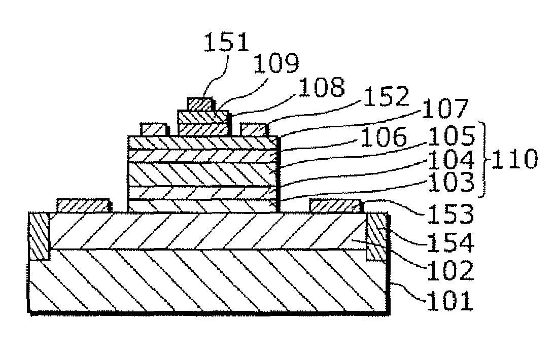
[0060]FIG. 6 is a cross-section diagram showing a structure of an HBT according to the first embodiment of the present invention.

[0061]As shown in FIG. 6, in this HBT, on a substrate 101 made of semi-insulating GaAs, a sub-collector layer 102, a collector layer 110, a base layer 106, an emitter layer 107, an emitter cap layer 108, and an emitter contact layer 109 are sequentially formed. The sub-collector layer 102 is made of n+-type GaAs doped with n-type impurity at a high concentration of 5×1018 cm−3. The collector layer 110 is doped with n-type impurity, and is formed on the sub-collector layer 102. The base layer 106 is formed on the collector layer 110, and is made of p-type GaAs of 100 nm in film thickness, doped with impurity at a high concentration of 4×1019 cm−3. The emitter layer 107 with a larger bandgap than the base layer 106 is formed on the base layer 106, and is made of InGaP doped with n-type impurity at an impurity concentration of 3×1017 cm−3. The collector layer...

second embodiment

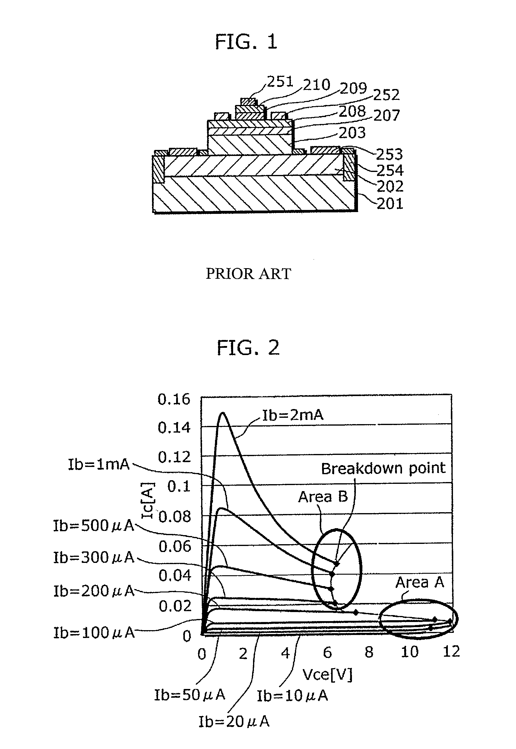
[0075]FIG. 8 is a cross-section diagram showing a structure of an HBT according to the second embodiment of the present invention.

[0076]As shown in FIG. 8, in this HBT, on the substrate 101 made of semi-insulating GaAs, the sub-collector layer 102, a collector layer 410, the base layer 106, the emitter layer 107, the emitter cap layer 108, and the emitter contact layer 109 are sequentially stacked. Here, the collector layer 410, the base layer 106, and the emitter layer 107 are processed to form a convex form, forming a base island region. The emitter cap layer 108 and the emitter contact layer 109 are stacked for forming a convex form, forming an emitter island region.

[0077]On a collector window formed where the first collector layer 403 is exposed, the collector electrode 153 made of AuGe / Ni / Au and the like is formed by evaporation. On the emitter contact layer 109, the emitter electrode 151 made of Pt / Ti / Pt / Au and the like is formed, and where the emitter layer 107 is exposed aro...


PUM

PropertyMeasurementUnit
thicknessaaaaaaaaaa
thicknessaaaaaaaaaa
thicknessaaaaaaaaaa

Abstract

The object of the present invention is to provide a heterojunction bipolar transistor with high breakdown tolerance which can be manufactured at a high reproducibility and a high yield, the heterojunction bipolar transistor includes: a sub-collector layer; a collector layer formed on the sub-collector layer; a base layer formed on the collector layer; and an emitter layer, which is formed on the base layer and is made of a semiconductor that has a larger bandgap than a semiconductor of the base layer, in which the collector layer includes: a first collector layer formed on the sub-collector layer; a second collector layer formed on the first collector layer; and a third collector layer formed between the second collector layer and the base layer, a semiconductor of the first collector layer differs from semiconductors of the third collector layer and the second collector layer, and an impurity concentration of the second collector layer is lower than an impurity concentration of the sub-collector layer and higher than an impurity concentration of the third collector layer.

Description

BACKGROUND OF THE INVENTION[0001](1) Field of the Invention[0002]The present invention relates to a heterojunction bipolar transistor, and particularly to an InGaP / GaAs heterojunction bipolar transistor.[0003](2) Description of the Related Art[0004]Heterojunction bipolar transistors (HBT) using semiconductor with large bandgap for emitter have been in practical use as high-frequency analogue elements for mobile phones and the like. In particular, an InGaP / GaAs HBT using InGaP as an emitter has small temperature dependency of current gain (HFE) since discontinuity of valence band (ΔEv) is large, and is expected to be widely used as a highly reliable device.[0005]A device structure of a general InGaP / GaAs HBT is described hereafter with reference to a diagram (for example, see Japanese Laid-Open Patent Application No. 2000-260783).[0006]FIG. 1 is a diagram showing a structure of an npn-type InGaP / GaAs HBT.[0007]As shown in FIG. 1, in the InGaP / GaAs HBT, an n+-type GaAs sub-collector l...

Claims


Application Information

Patent Timeline
Patent Type & Authority Patents(United States)
IPC IPC(8): H01L29/739
CPCH01L29/0821H01L29/7371H01L29/66318
Inventor MURAYAMA, KEIICHITAMURA, AKIYOSHIMIYAMOTO, HIROTAKAMIYAJIMA, KENICHI
Owner PANASONIC SEMICON SOLUTIONS CO LTD
Why Eureka
Try Eureka