Method and system for memory testing and test data reporting during memory testing

a memory and data technology, applied in the field of memory testing, can solve problems such as flagging memory as unrepairable, and achieve the effects of reducing the number of pins used or necessary, narrowing the interface, and reducing the cost of the chip

Active Publication Date: 2010-06-08
MARVELL ASIA PTE LTD
View PDF30 Cites 37 Cited by
  • Summary
  • Abstract
  • Description
  • Claims
  • Application Information

AI Technical Summary

Benefits of technology

[0015]It is also an object of the present invention to reduce the number of pins used or necessary for memory testing. In accordance with this aspect, as a result of the efficient error reporting method of the present invention, the invention uses fewer pins for data transfer between the BIST and the external memory tester, thus providing a narrower interface and reducing chip cost.

Problems solved by technology

If the number of reported failures exceeds the available redundant resources, the BIST will flag the memory as unrepairable.

Method used


Image

  • Method and system for memory testing and test data reporting during memory testing
  • Method and system for memory testing and test data reporting during memory testing
  • Method and system for memory testing and test data reporting during memory testing

Examples


second embodiment

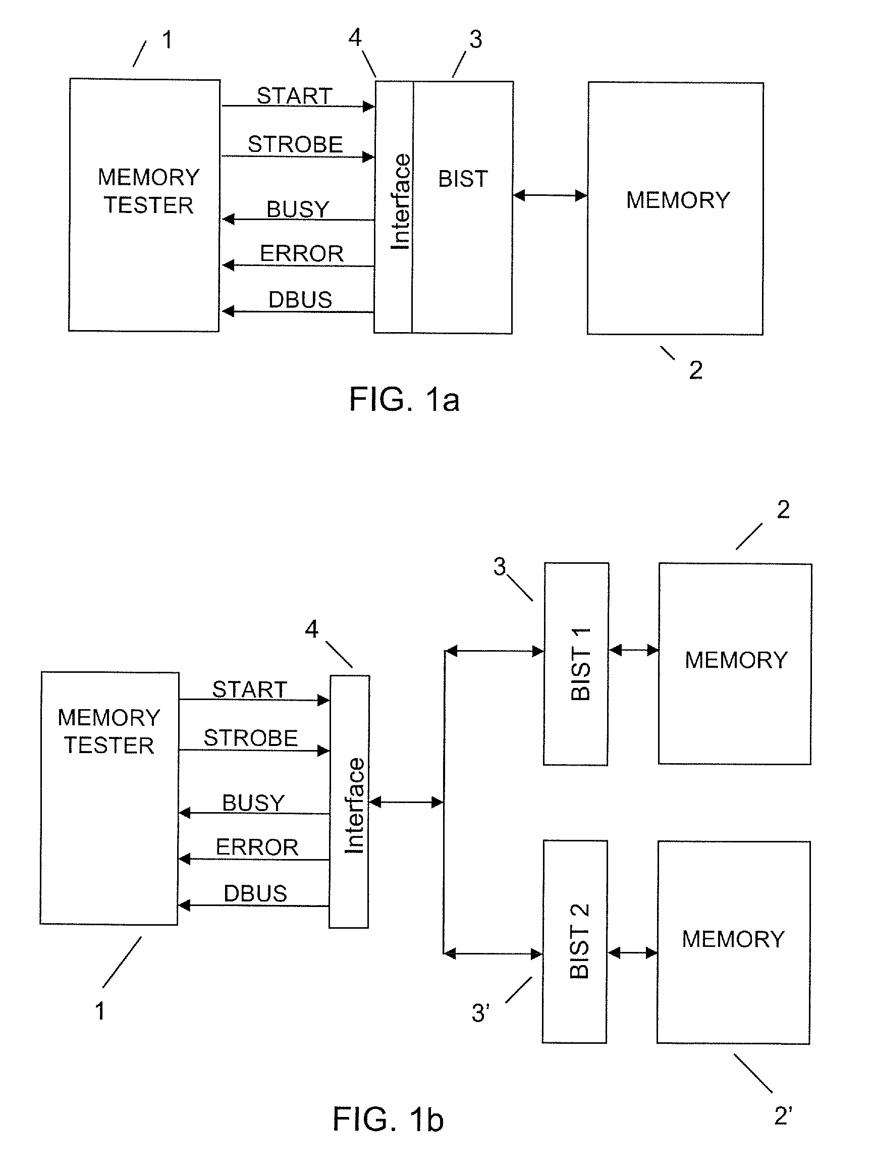
[0044]Looking now at FIG. 1b, which shows the memory testing system of the present invention, memories 2 and 2′ are coupled to BIST 3 and BIST 3′ respectively, which in turn are coupled to the interface 4. In this embodiment, a single memory tester 1 can test multiple memories, 2, 2′. Similarly to the memory testing system shown in FIG. 1a, the interface 4 in this embodiment communicates with the memory tester 1 via the following signals: START, STROBE, BUSY, ERROR, DBUS. A variation of this embodiment is to couple multiple embedded memories to one BIST, which is coupled to the interface 4.

third embodiment

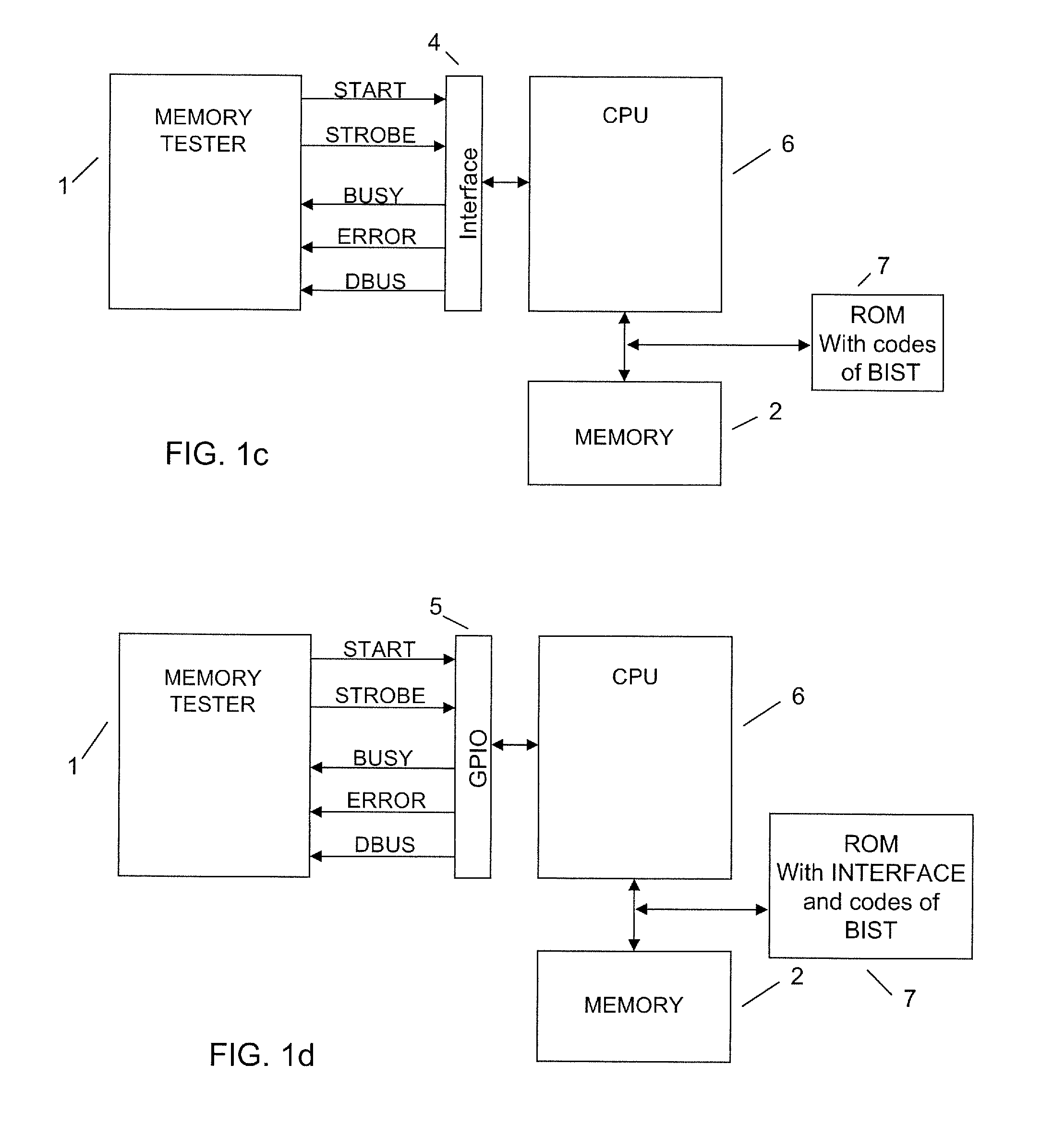
[0045]FIG. 1c shows the memory testing system of the present invention, in which a CPU 6, or other processor, extracts failed memory location information from the memory, instead of BIST 3. Test patterns are loaded into the instruction memory for the CPU 6. The CPU 6 then executes the instructions from the instruction memory and tests the memory 2. The CPU 6 is coupled to the interface 4, which communicates with the memory tester 1.

fourth embodiment

[0046]FIG. 1d shows the memory testing system of the present invention, in which a general processor input / output interface (GPIO) replaces the interface 4 in the memory testing system shown in FIG. 1c. GPIO is an existing standard interface. Like the interface 4 in the memory testing systems shown in FIGS. 1a, 1b, and 1c, GPIO communicates with the memory tester 1 via signals START, STROBE, BUSY, ERROR and DBUS. This embodiment is an example of using an existing interface to implement the present invention. GPIO could be used with a BIST instead of a CPU.

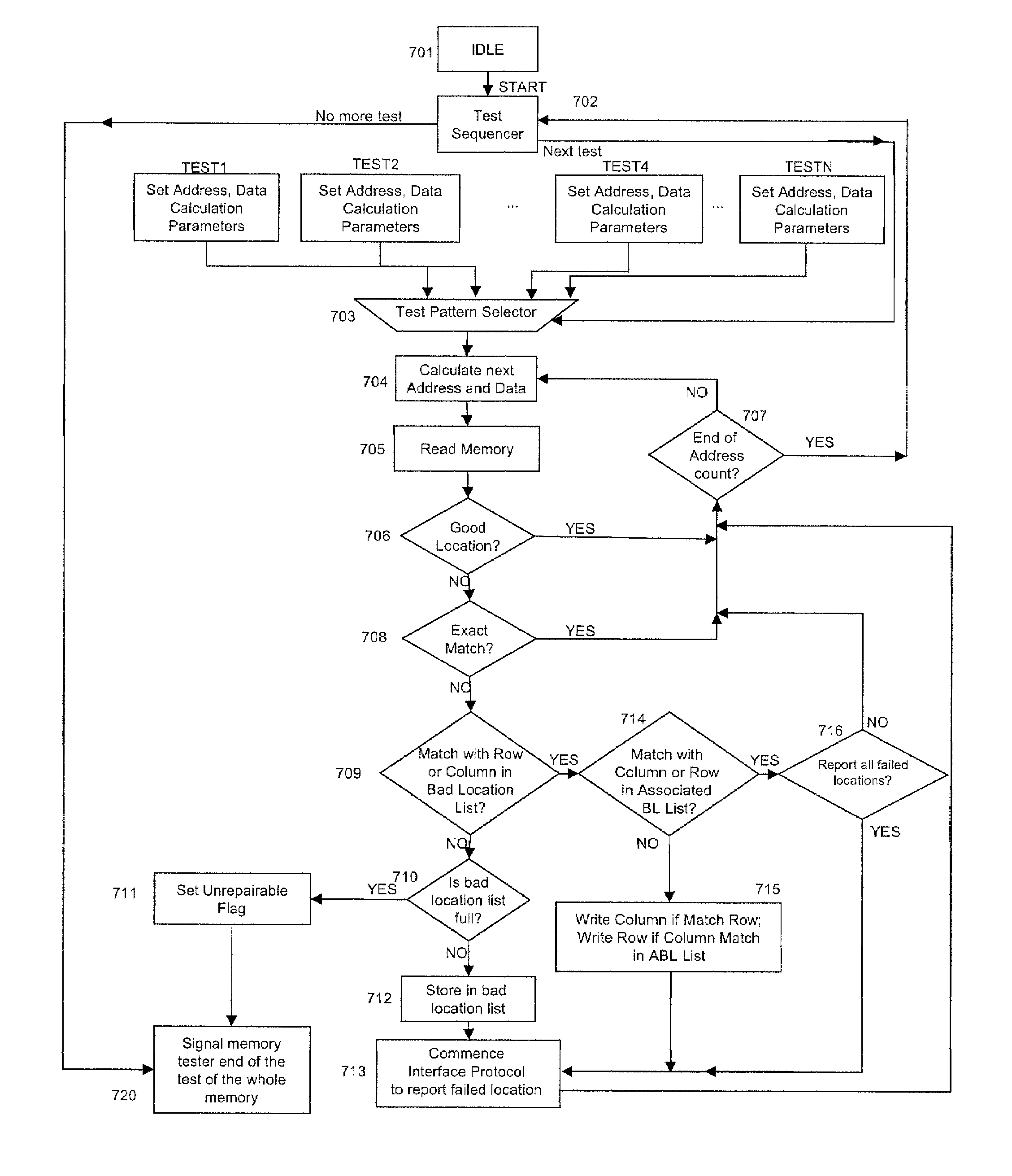
[0047]The interface protocol of the present invention provides a handshake between the memory tester 1 and the BIST 3, but does not in any way change or limit the memory tester, the BIST, or the memory testing mechanism inside the chip. The BIST can have many different functions, and generate all kinds of different test patterns. As mentioned above, a CPU can replace the BIST to extract the failed memory location information from t...


PUM


Abstract

The present invention provides a method and system for improving memory testing efficiency, raising the speed of memory testing, detecting memory failures occurring at the memory operating frequency, and reducing data reported for redundancy repair analysis. The memory testing system includes a first memory tester extracting failed memory location information from the memory at a higher memory operating frequency, an external memory tester receiving failed memory location information at a lower memory tester frequency, and an interface between the first memory tester and the external memory tester. The memory testing method uses data strobes at the memory tester frequency to clock out failed memory location information obtained at the higher memory operating frequency. In addition, the inventive method reports only enough information to the external memory tester for it to determine row, column and single bit failures repairable with the available redundant resources. The present invention further provides a redundant resource allocation system, which uses a bad location list and an associated bad location list to classify failed memory locations according to a predetermined priority sequence, and allocates redundant resources to repair the failed memory locations according to the priority sequence.

Description

CROSS-REFERENCE TO RELATED APPLICATIONS[0001]This application is a divisional application of U.S. application Ser. No. 10 / 734,420 filed Dec. 11, 2003, which claims the benefit of Provisional Application No. 60 / 436,805, filed Dec. 26, 2002. This application incorporates both of these applications by reference.BACKGROUND OF THE INVENTION[0002]1. Field of the Invention[0003]The present invention relates to memory testing, and more specifically to efficiently testing and reporting failed memory locations as well as to efficiently allocating redundant resources to repair defective memory locations.[0004]2. Description of the Related Art[0005]One of the first steps in memory repairing is to determine failed memory locations, usually by writing data to an array of memory locations, reading data from those memory locations, and then comparing the read data to the data previously written to determine failed memory locations.[0006]Memory testing has involved using an external memory tester wi...

Claims


Application Information

Patent Timeline
Patent Type & Authority Patents(United States)
IPC IPC(8): G11C29/00
CPCG11C29/12015G11C29/14G11C29/16G11C29/00G11C29/48G11C29/44G11C2029/1208G11C2029/5602G06F11/2094G11C29/12G11C29/4401G11C29/56G11C29/72
Inventor LEE, WINSTONWU, ALBERTLIOU, CHORNG-LII
Owner MARVELL ASIA PTE LTD
Why Eureka
Try Eureka