Semiconductor device and program data redundancy method therefor
a technology of program data and semiconductors, applied in the field of semiconductor devices, can solve the problem that already written data cannot be secured, and achieve the effect of increasing system reliability, data can be secured, and data loss prevention
- Summary
- Abstract
- Description
- Claims
- Application Information
AI Technical Summary
Benefits of technology
Problems solved by technology
Method used
Image
Examples
first embodiment
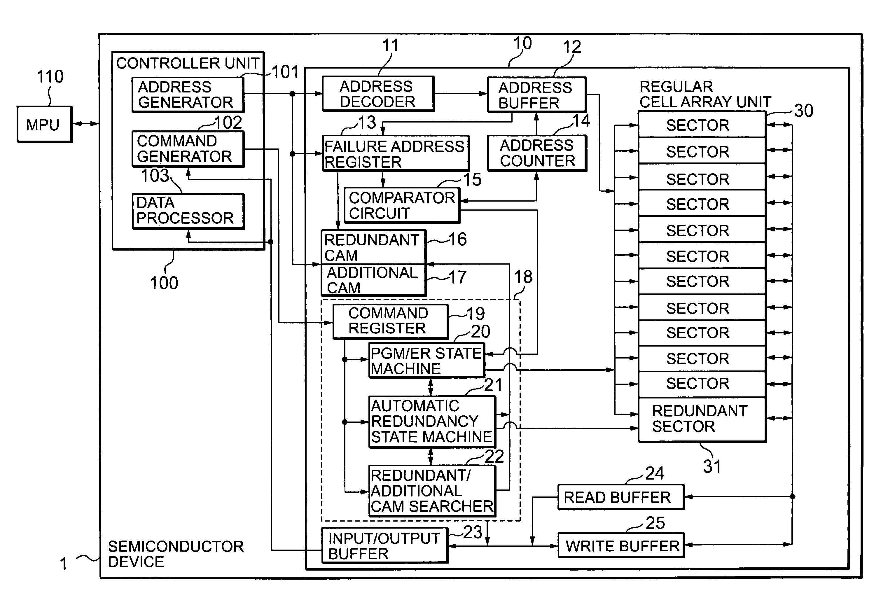
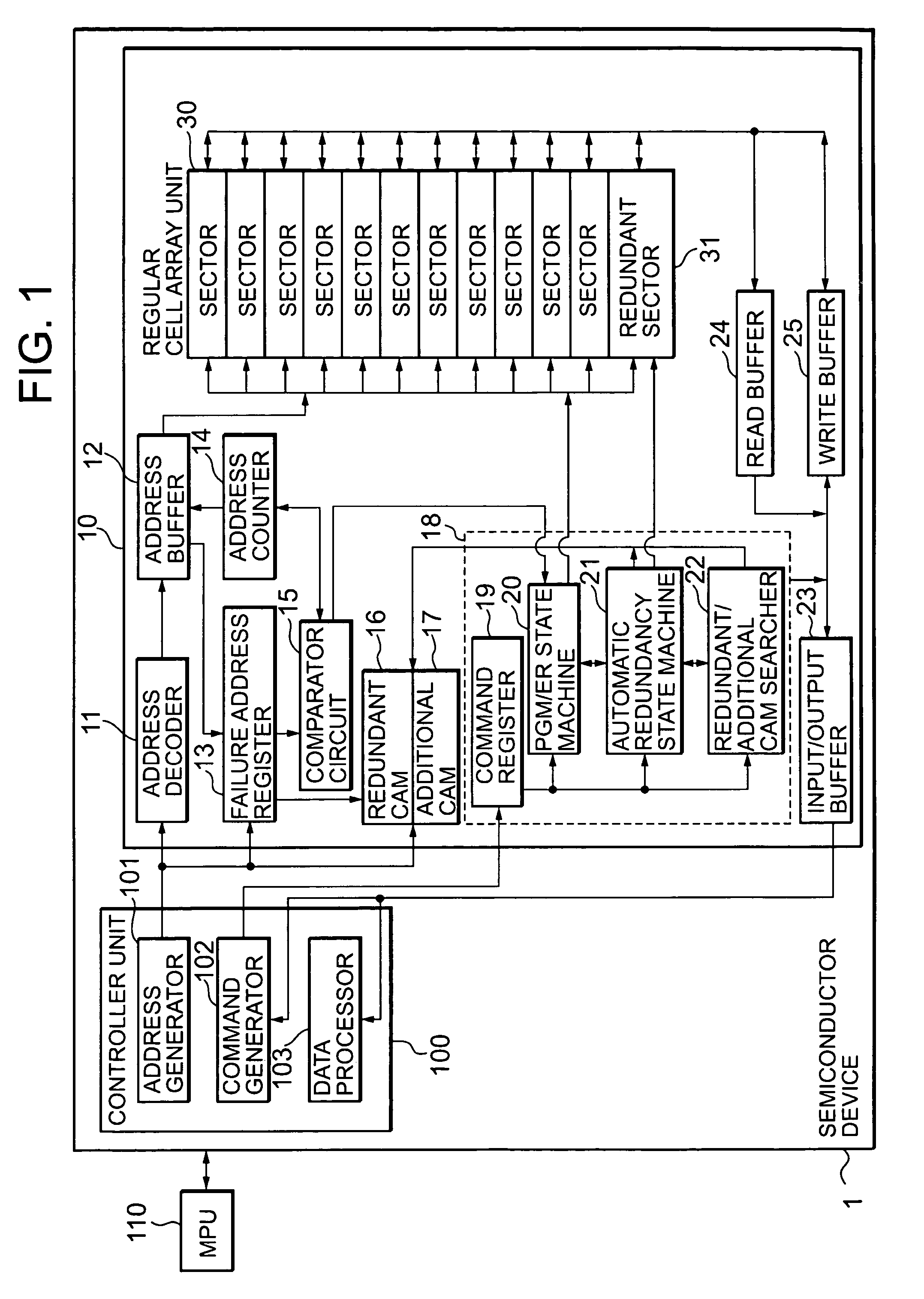
[0024]Referring first to FIG. 1, a structure of a semiconductor device in accordance with a first embodiment of the present invention is described. As shown in FIG. 1, a semiconductor device 1 in accordance with the first embodiment includes a memory unit 10 and a controller unit 100 that controls the memory unit 10. A Micro Processing Unit (MPU) 110 that controls the semiconductor device 1 is connected to the semiconductor device 1 from outside.
[0025]The controller unit 100 includes an address generator 101, a command generator 102, and a data processor 103, as shown in FIG. 1. The address generator 101 generates addresses of a cell array unit in which data is to be written or erased. The command generator 102 analyzes instructions input from the external MPU 110 and generates commands such as programming commands and erasing commands. Each generated command is output to a command register 19 of the memory unit 10. The data processor 103 processes data to be written into the memory...
second embodiment
[0071]In accordance with a second embodiment of the present invention, a semiconductor device illustrated in FIG. 10 can be employed. The semiconductor device illustrated in FIG. 10 includes a regular sector 121 and a redundant sector 122 connected to separate data bus lines 131 and 132, respectively. Also, a read sense amplifier 123 and a redundancy sense amplifier 124 are provided independently of each other and coupleable to a read buffer 127 and a write buffer 128 by switches 125 and 126, respectively. With this structure, a redundant cell array unit can be provided at any location outside the array. Also, since the flow of data is unidirectional, the time required for operations such as switching can be shortened.
third embodiment
[0072]In accordance with the third embodiment for the present invention, as illustrated in FIGS. 11A and 11B, the data of the sector in which an error has occurred is stored in a latch circuit 141 connected to a bit line in a NAND-type flash memory. In FIG. 11A, a switch 142 is provided to switch the applied voltage between a programming voltage and an erasing voltage for the sector. In FIG. 11B, the latch circuit 141 is connected directly to a bit line, and a PGM voltage converter 143 that applies a voltage to the bit line adjusts the voltages to be applied.
[0073]The above described embodiments are preferred embodiments of the present invention. However, the present invention is not limited to these embodiments, and various changes may be made to them within the scope of the present invention. For example, a row address and a column address are compared with each other so as to determine the memory cell in which an error has occurred and write the data into the redundant sector in ...
PUM
 Abstract
Description
Claims
Application Information


