RF power amplifier

a power amplifier and amplifier technology, applied in the direction of rf amplifiers, supply voltage varying control, transmission, etc., can solve the problems of inability to improve the efficiency of the amplifier apparatus working at a middle output level or lower, the control system of a portable terminal and/or the entire system thereof can be significantly affected, and the power gain can change rapidly, etc., to achieve the effect of increasing the efficiency of the high-frequency power amplifier, increasing efficiency, and increasing efficiency

Active Publication Date: 2010-07-13
RENESAS ELECTRONICS CORP
View PDF6 Cites 44 Cited by
  • Summary
  • Abstract
  • Description
  • Claims
  • Application Information

AI Technical Summary

Benefits of technology

[0019]In accordance with a technique described in Patent Document 1, a high-frequency power amplifier apparatus 1400 has a structure as shown in FIG. 34. Specifically, in the amplifier apparatus, the following means is adopted for amplifiers connected in parallel in order to make the Doherty amplifier effective as a linear amplifier. That is, the bias for the carrier amplifier 1410 is fixed, while only the bias for the peaking amplifier 1411 is switched at a predetermined threshold in accordance with an input signal power, whereby the linearity is improved.

Problems solved by technology

Therefore, the frequent changes in input power near the previously defined threshold cause the frequent switching of the bias, which leads to the rapid changes in power gain, current, phase and the like.
As a result, the control system of a portable terminal and / or the entire system thereof can be affected significantly.
In addition, there is a problem such that the efficiency of the amplifier apparatus working at a middle output level or lower cannot be improved only by changing the bias of one amplifier.
However, the techniques have a problem that the frequent changes in amount of input power near the predetermined threshold produce the rapid changes in power gain, power-added efficiency, phase difference, etc.

Method used


Image

  • RF power amplifier
  • RF power amplifier
  • RF power amplifier

Examples


embodiment a

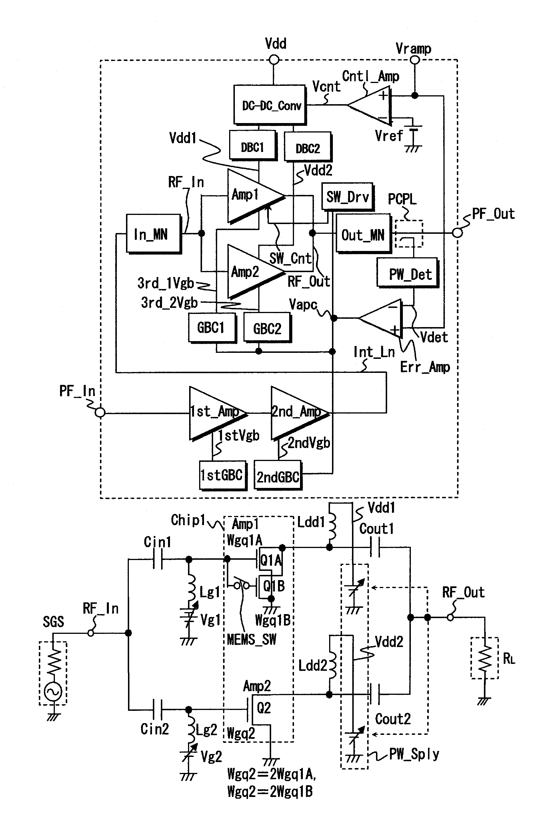
[0170]FIG. 18 is a block diagram showing a high-frequency power amplifier of Embodiment A in association with the invention. The high-frequency power amplifier 100 of Embodiment A includes: a plurality of power amplifiers (AMP1) 110 and (AMP2) 111 disposed in parallel (two power amplifiers are exemplified here); and a plurality of bias control circuits (Bias_cont1) 112 and (Bias_cont2) 113, each controlling corresponding one of the plurality of power amplifiers 110 and 111 in bias in accordance with a method of modulating an input signal, which are formed on a monolithic board. The power amplifiers 110 and 111 each have an input terminal connected to a high-frequency signal input terminal 101 through a signal distributing part, and an output terminal connected to a high-frequency signal output terminal 102 through a signal synthesizing part. The bias control circuits 112 and 113 each have an input terminal connected to a modulation signal information input terminal 105, and an outpu...

embodiment b

[0176]FIG. 21 is a block diagram showing a high-frequency power amplifier in accordance with Embodiment B of the invention. The high-frequency power amplifier 200 in accordance with this embodiment includes: power amplifiers (AMP1) 210 and (AMP2) 211; bias control circuits (Bias_cont1) 212 and (Bias_cont2) 213; a high-frequency signal input terminal 201; and a high-frequency signal output terminal 202. Further, the high-frequency power amplifier has an RF_IC part (MOD RF_IC) 214 including a signal modulation part and a signal source (Signal) 215 connected thereto from the outside.

[0177]In the high-frequency power amplifier 200 in accordance with this embodiment, the RF_IC part 214 including the signal modulation part offers modulation signal information. A high-frequency signal to be input to the high-frequency signal input terminal 201 of the high-frequency power amplifier 200 is sent from the external signal source 215 through the RF_IC part 214 to the input terminal. Other operat...

embodiment c

[0179]FIG. 22 is a block diagram showing a high-frequency power amplifier in accordance with Embodiment C of the invention. The high-frequency power amplifier 300 in accordance with this embodiment includes: power amplifiers (AMP1) 310 and (AMP2) 311; bias control circuits (Bias_cont1) 312 and (Bias_cont2) 313; distributed parameter lines (TRL_IN1) 303, (TRL_OUT1) 304, and (TRL_OUT2) 305; a high-frequency signal input terminal 301; and a high-frequency signal output terminal 302. Further, the high-frequency power amplifier has an RF_IC part (MOD RF_IC) 314 including a signal modulation part and a signal source (Signal) 315 connected thereto from the outside.

[0180]As for the high-frequency power amplifier 300 in accordance with this embodiment, as in the case of Embodiment B shown in FIG. 21, a high-frequency signal to be input to the high-frequency signal input terminal 301 is sent from the external signal source 315 through the RF_IC part 314 including the signal modulation part to...


PUM


Abstract

The RF power amplifier includes first and second amplifiers Q1 and Q2 as final-stage amplification power devices connected in parallel between an input terminal RF_In and an output terminal RF_Out. The amplifiers Q1 and Q2 are formed on one semiconductor chip. The first bias voltage Vg1 of the amplifier Q1 is set to be higher than the second bias voltage Vg2 of the amplifier Q2 so that the amplifier Q1 is operational between Class B and AB, and Q2 is operational in Class C. The first effective device size Wgq1 of the amplifier Q1 is intentionally set to be smaller than the second effective device size Wgq2 of the amplifier Q2 beyond a range of a manufacturing error of the semiconductor chip. An RF power amplifier that exhibits a high power-added efficiency characteristic regardless of whether the output power is High or Low can be materialized.

Description

CLAIM OF PRIORITY[0001]The present application claims priority from Japanese applications JP 2006-168285 filed on Jun. 19, 2006, JP 2006-175374 filed on Jun. 26, 2006 and JP 2007-145009 filed on May 31, 2007, the contents of which are hereby incorporated by reference into this application.FIELD OF THE INVENTION[0002]The present invention relates to an RF power amplifier for RF transmission, which is incorporated in a communication terminal tool such as a portable phone terminal for communicating with a base station, or which is used in a base station. Particularly, it relates to a technique profitable to improve the power efficiency by means of two or more final-stage amplification power devices in the RF power amplifier. The term, high-frequency power amplifier is herein equivalent to the term, RF power amplifier.BACKGROUND OF THE INVENTION[0003]Various communication systems are used in the world presently. Such communication systems are not necessarily the same because old and new...

Claims


Application Information

Patent Timeline
Patent Type & Authority Patents(United States)
IPC IPC(8): H01Q11/12
CPCH03F1/0266H03F1/0277H03F1/0288H03F3/195H03F3/211H03G3/004H03F2200/108H03F2200/181H03F2200/432H03F2200/451H03F2200/456H04B2001/045H03F1/02H03F3/24
Inventor FUJIOKA, TORUSHIMIZU, TOSHIHIKOOHNISHI, MASAMIMATSUMOTO, HIDETOSHITANAKA, SATOSHI
Owner RENESAS ELECTRONICS CORP
Why Eureka
Try Eureka