Electrically alterable memory cell

a memory cell, electrically programmable technology, applied in the direction of semiconductor devices, electrical apparatus, transistors, etc., to achieve the effect of suppressing the large c

Inactive Publication Date: 2010-07-20
MARVELL ASIA PTE LTD
View PDF121 Cites 4 Cited by
  • Summary
  • Abstract
  • Description
  • Claims
  • Application Information

AI Technical Summary

Benefits of technology

[0008]Briefly, another preferred embodiment of the present invention is a nonvolatile memory cell. A body of a semiconductor material is provided having a first conductivity type. A first and a second region of a second conductivity type are formed in the body, and between them create a channel region in the body. A charge storage layer is disposed over and insulated from the channel region. A ballistic gate and a supplier gate are further provided, next to each other and insulated from the charge storage layer, with the supplier gate being of a second semiconductor material and having an energy band gap and impurity concentration different from the ballistic gate. A tunneling gate is then disposed over and insulated from the uppermost of the ballistic gate and the supplier gate by a charge filter.
Summary On Advantages Of The Present Invention:
[0011]2) The present invention provides the filter structure permitting thicker dielectrics be used in the cell. A thicker dielectric has the advantage on manufacturing control, thus the memory cell of the present invention is more manufacturable than cells without the filter structure;
[0010]The cells provided in the present invention illustrate that the requirement on a large work function for the ballistic gate, as required for minimizing parasitic charges, is not necessary. Further, the cell structures of the present invention remove the requirement on maintaining a similar current level for the forward and the backward tunneling carriers. The backward tunneling current can be reduced by the filter to fix the current waste problem;
[0011]2) The present invention provides the filter structure permitting thicker dielectrics be used in the cell. A thicker dielectric has the advantage on manufacturing control, thus the memory cell of the present invention is more manufacturable than cells without the filter structure;
[0012]3) The present invention permits erase operation without suffering dielectric breakdown problem;
[0013]4) The present invention avoids impact ionization in ballistic gate and in tunneling gate;
[0014]5) The present invention permits cell operation without cell disturb, and provide cell structure more effective on cell disturb prevention in un-selected cells;
[0015]6) The present invention suppresses large R effect and permits lower sheet-resistance polysilicon (i.e. n-type poly) for ballistic gate and tunneling gate, made possible by removing the restriction on material selection (e.g. p-type polysilicon) for ballistic gate or by providing an unique energy band architecture on supply gate and ballistic gate in cells of present invention; and
[0016]7) The present invention suppresses large C effect;
[0017]These and other objects and advantages of the present invention will become clear to those skilled in the art in view of the description of the preferred embodiment as described herein and as illustrated in the figures of the drawings.

Problems solved by technology

However, there are several fundamental problems associated with the energy band structure of transistor in the noted article when employed for the ballistic transport mechanism.
Further, there are fundamental problems when such mechanism and band structure are considered for non-volatile memory operation.

Method used


Image

  • Electrically alterable memory cell
  • Electrically alterable memory cell
  • Electrically alterable memory cell

Examples


embodiment 100

Embodiment 100

[0047]As used herein, the symbol n+ indicates a heavily doped n-type semiconductor material typically having a doping level of n-type impurities (e.g. arsenic) on the order of 1020 atoms / cm3. The symbol p+ indicates a heavily doped p-type semiconductor material typically having a doping level of p-type impurities (e.g. boron) on the order of 1020 atoms / cm3.

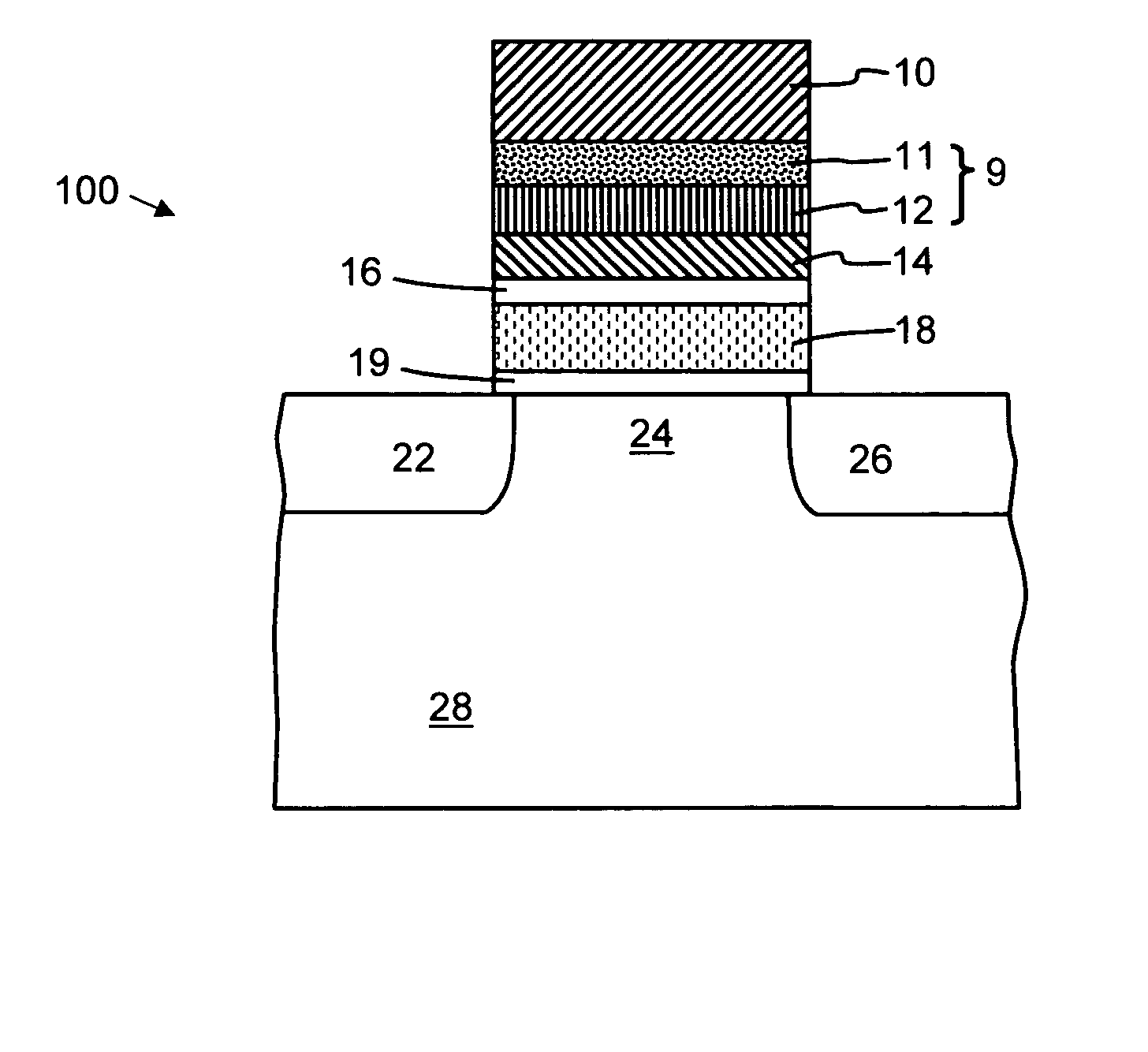
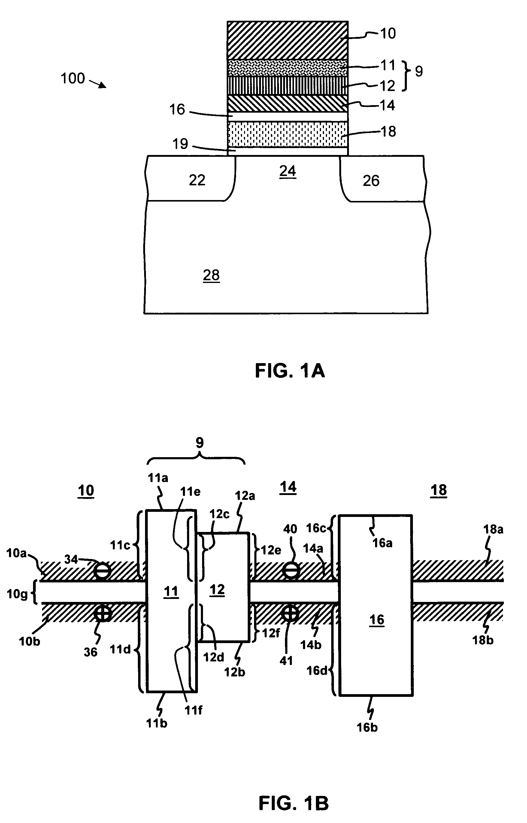
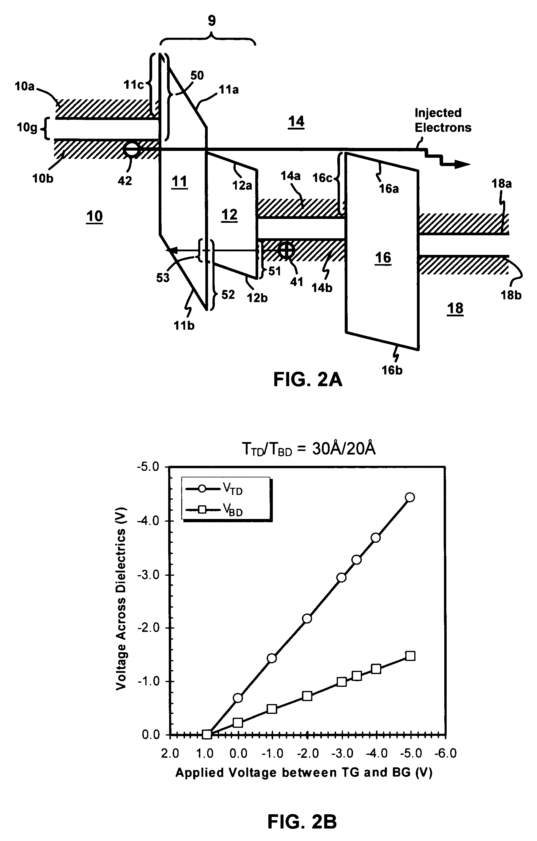
[0048]FIG. 1A shows a cross-sectional view of cell architecture 100 in accordance with one embodiment of the present invention. There is shown a tunneling gate (TG 10), a filter 9, a ballistic gate (BG 14), a floating gate (FG 18), a source 22, a channel 24, a drain 26, and a body 28 in a semiconductor substrate (such as a silicon substrate or a silicon-on-insulator substrate). The filter 9 comprises a tunneling dielectric (TD 11) and a blocking dielectric (BD 12). The TD 11 is sandwiched in between the TG 10 and the BD 12 regions. Likewise, the BD 12 is sandwiched in between the TD 11 and the BG 14 regions. The BG 1...

embodiment 200

Embodiment 200

[0128]FIGS. 11A and 11B provide respectively a cell structure 200 and an energy band diagram in the flat-band condition for another embodiment of the present invention. The memory cell 200 of FIG. 11A is similar to the one illustrated in FIG. 1A except with a difference on the filter 9 structure in between TG 10 and BG 14. These differences are described herein. Referring to FIG. 11A, there is shown a filter 9 comprising an upper tunneling dielectric (UTD 71), a lower tunneling dielectric (LTD 72), and a blocking material (BM 73) disposed therebetween. The UTD 71 can be a dielectric material such as oxide or any other materials considered in connection with TD 11 of cell 100. The LTD 72 can be a dielectric having a lower energy gap and a higher dielectric constant than that of UTD 71. In general, the materials for UTD 71 and LTD 72 should be high quality dielectrics permitting charge carriers to transport therethrough from one side of the dielectric to the other in qua...

embodiment 300

Embodiment 300

[0133]Provided in FIG. 12A is a similar cell structure as in FIG. 11A except by replacing the BM 73 of FIG. 11A with a plurality of blocking nano-crystals (BNC 74) each having energy gap comparable or larger than that of TG 10. The BNC 74 can be in a ball shape with a diameter in the range comparable to the wavelength of charge carriers (i.e. electrons or holes). Typical range of the diameter is about 30 Å to about 200 Å. The nano-crystals 74 can be formed by Ultra-High-Vacuum Chemical-Vapor-Deposition (“UHVCVD”) technique well-known in the art. The nano-crystal functions as an “island” between TG 10 and BG 14 to permit charge carriers hopping therethrough. In specific, as a proper bias is applied between TG 10 and BG 14, charge carriers in TG 10 are emitted through tunneling mechanism onto BNC 74 and subsequently tunneling into the BG 14. The cell structure comprises two types of zone. The first type of zone contains a nano-crystal 74 in between TG 10 and BG 14 (for e...


PUM


Abstract

A nonvolatile memory cell is provided. The cell has a charge filter, a tunneling gate, a ballistic gate, a charge storage layer, a source, and a drain with a channel defined between the source and drain. The charge filter permits transporting of charge carriers of one polarity type from the tunneling gate through the blocking material and the ballistic gate to the charge storage layer while blocking the transport of charge carriers of an opposite polarity from the ballistic gate to the tunneling gate. Further embodiments of the present invention provide a cell having a charge filter, a supplier gate, a tunneling gate, a ballistic gate, a source, a drain, a channel, and a charge storage layer. The present invention further provides an energy band engineering method permitting the memory cell be operated without suffering from disturbs, from dielectric breakdown, from impact ionization, and from undesirable RC effects.

Description

RELATED APPLICATIONS[0001]This application claims the benefit of U.S. Provisional Application No. 60 / 585,238, filed Jul. 1, 2004.TECHNICAL FIELD[0002]The present invention deals with nonvolatile memory, and relates more specifically to Electrically Programmable Read Only Memories (EPROM) and Electrically Erasable and Programmable Read Only Memories (EEPROM). More particularly, the present invention relates to memory cell structure and method altering barrier heights of ballistic-charge filter for memory cell operations.BACKGROUND OF THE INVENTION[0003]Non-volatile semiconductor memory cells permitting charge storage capability are well known in the art. The charges are typically stored in a floating gate to define the states of a memory cell. Typically, the states can be either two levels or more than two levels (for multi-level states storage). Mechanisms such as channel hot electron (CHE), source-side injection (SSI), Fowler-Nordheim tunneling (FN), and Band-to-Band Tunneling (BTB...

Claims


Application Information

Patent Timeline
Patent Type & Authority Patents(United States)
IPC IPC(8): H01L29/786
CPCH01L29/42324H01L29/7881H01L29/7883H01L29/792
Inventor WANG, CHIH-HSIN
Owner MARVELL ASIA PTE LTD
Why Eureka
Try Eureka