Semiconductor substrate including first and second recognition marks and method for manufacturing semiconductor device

a semiconductor and substrate technology, applied in the direction of semiconductor devices, semiconductor/solid-state device details, electrical equipment, etc., can solve the problems of difficult to make a shape having a fine pattern shape, the accuracy of the method is inferior to the processing accuracy of the dicing wafer process, and the dimensional tolerance required in the manufacturing process of the semiconductor package has become much severer. , to achieve the effect of miniaturizing the semiconductor device, reducing the dimensional tolerance of the semiconductor substrate, and improving the detection accuracy

Inactive Publication Date: 2010-07-20
LONGITUDE SEMICON S A R L
View PDF14 Cites 1 Cited by
  • Summary
  • Abstract
  • Description
  • Claims
  • Application Information

AI Technical Summary

Benefits of technology

[0013]In one embodiment, there is provided a first semiconductor substrate according to the present invention comprises: a plurality of semiconductor elements which are arrayed in a matrix form and which are implemented thereon; a dividing line for cutting the plurality of the implemented semiconductor elements into the individual elements and separating them; a first recognition mark which is arranged in the frame part of the perimeter of the implementation region having a plurality of semiconductor elements implemented therein so that the position of the semiconductor substrate can be macroscopically detected by detecting means; and a second recognition mark which is formed into a smaller shape than the first recognition mark so that the position of the dividing line can be microscopically detected by detecting means. The second recognition mark is arranged so that its center line is positioned on a line that extends from the dividing line, and has a pattern shape which is formed so as to be linearly symmetric with respect to the center line. The pattern shape is formed so that the ratio in a direction parallel to the dividing line is larger than that in a direction perpendicular to the dividing line, and includes a flow region for promoting the flow of the etchant in order to form the pattern shape.
[0016]The manufacturing method according to the present invention can improve detection accuracy for detecting the position of a second recognition mark having a fine pattern shape. Accordingly, the manufacturing method according to the present invention can decrease the dimensional tolerance of a semiconductor substrate and miniaturize a semiconductor device.

Problems solved by technology

Along with the increase, dimensional tolerance required in the manufacturing process of the semiconductor package has become much severer.
Therefore, the accuracy in the method is shown to be inferior to the processing accuracy in a process of dicing wafers when a recognition camera that has high magnification is caused to recognize the dicing position.
Accordingly, it is difficult to make a shape having a fine pattern shape with such accuracy that the pattern center can be stably detected.
When the sag is formed in the pattern shape configuring the recognition mark, the camera cannot stably recognize the position of the pattern center, which causes the misalignment of the dicing position of the wiring board.
However, when the recognition mark is formed to have a fine pattern shape in the step of forming the wiring pattern on the substrate, the pattern shape in the recognition mark will vary and consequently becomes unusable as the pattern shape.
Then, it is difficult to employ a method of detecting the position by using a recognition camera having high magnification in the step of dicing the substrate, and accordingly it is necessary to secure large dimensional tolerance, which prevents miniaturization of the semiconductor package.
The recognition mark disclosed in the above described Patent document 1 has a problem in which the a corner part of the pattern shape which is formed into a rectangle is dissolved in the etchant which causes the pattern shape to easily break which causes the recognition mark be barely detectable.
In addition, the pattern shape of the recognition mark is formed into a rectangle which is similar to the wiring pattern formed on the wiring board, which causes a problem that one part of the wiring pattern is easy to be wrongly recognized as the recognition pattern.

Method used


Image

  • Semiconductor substrate including first and second recognition marks and method for manufacturing semiconductor device
  • Semiconductor substrate including first and second recognition marks and method for manufacturing semiconductor device
  • Semiconductor substrate including first and second recognition marks and method for manufacturing semiconductor device

Examples


Embodiment Construction

[0027]The invention will be now described herein with reference to illustrative embodiments. Those skilled in the art will recognize that many alternative embodiments can be accomplished using the teachings of the present invention and that the invention is not limited to the embodiments illustrated for explanatory purposes.

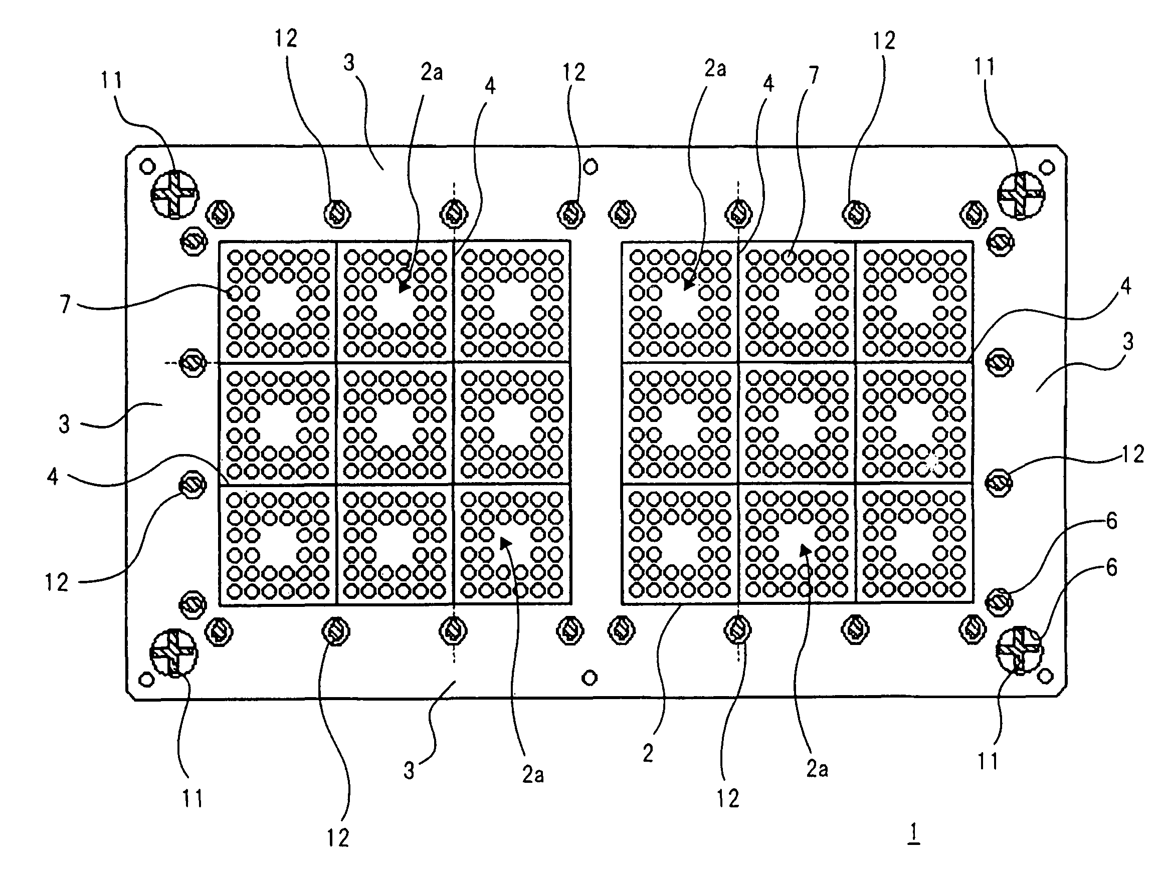
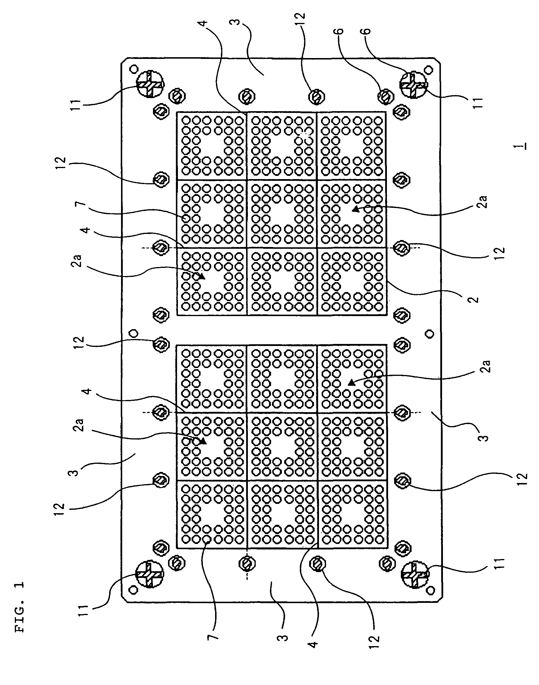
[0028]FIG. 1 illustrates a plan view of semiconductor packaging substrate 1 according to a first exemplary embodiment. Referring now to FIG. 1, semiconductor packaging substrate 1 according to a first embodiment of the present invention includes: implementation region 2 in which a plurality of semiconductor chips are arrayed in a matrix form and implemented; frame part 3 that forms a quadrangle arranged in the perimeter of implementation region 2; and a plurality of dicing lines 4 (dividing line) for cutting a plurality of the semiconductor chips which are implemented in implementation region 2 into individual chips and for separating them.

[0029]In implementation...


PUM


Abstract

The present invention includes a first recognition mark which is arranged in a frame part of a perimeter of an implementation region having a plurality of semiconductor chips implemented therein so that the position of the semiconductor substrate can be macroscopically detected by using a recognition camera, and a second recognition mark which is formed into a smaller shape than the first recognition mark so that the position of the dividing line can be microscopically detected by using a recognition camera. The second recognition mark is arranged so that its center line is positioned on a line that extends from a dicing line, and has a pattern shape which is formed so as to be linearly symmetric with respect to the center line. This pattern shape is formed so that the ratio of a length occupying a direction parallel to the dicing line is larger than that occupying a direction perpendicular to the dicing line, and includes a flow region for promoting the flow of an etchant for forming the pattern shape.

Description

BACKGROUND OF THE INVENTION[0001]1. Field of the Invention[0002]The present invention relates to a semiconductor substrate having a plurality of semiconductor elements arrayed and implemented thereon in a manufacturing process of a semiconductor device, and a method for manufacturing a semiconductor device using the semiconductor substrate.[0003]2. Description of the Related Art[0004]In recent years, the requirement has arisen for semiconductor device (hereinafter referred to as a semiconductor package) is required to be miniaturized so that they can be mounted on a small electronic equipment such as a portable telephone. For this reason, in a BGA (Ball Grid Array) type of a semiconductor package, miniaturizing the semiconductor package is proceeded by making a wiring board having a semiconductor element (hereinafter referred to as a semiconductor chip) that is to be mounted thereon smaller.[0005]Thus, a semiconductor package which is formed into a size approximately equal to that o...

Claims


Application Information

Patent Timeline
Patent Type & Authority Patents(United States)
IPC IPC(8): H01L23/544H01L21/76H01L21/00
CPCH01L23/544H01L24/97H01L21/561Y10S438/975H01L24/85H01L2221/68331H01L2223/5442H01L2223/54426H01L2223/54473H01L2224/48091H01L2224/48227H01L2224/97H01L2924/15184H01L2924/15311H01L23/3128H01L2224/85H01L2924/01033H01L2924/01006H01L2924/01005H01L24/48H01L2924/00014H01L2924/181H01L2924/00012H01L2224/45099H01L2224/45015H01L2924/207
Inventor KINDO, OSAMU
Owner LONGITUDE SEMICON S A R L
Why Eureka
Try Eureka