

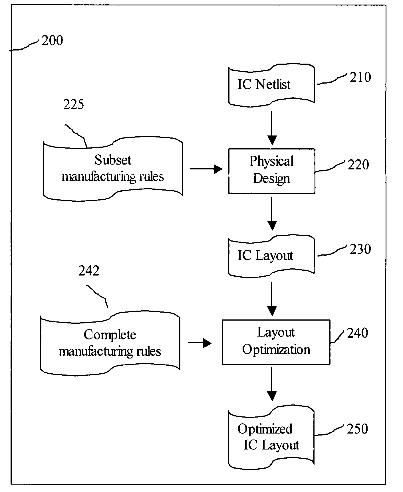
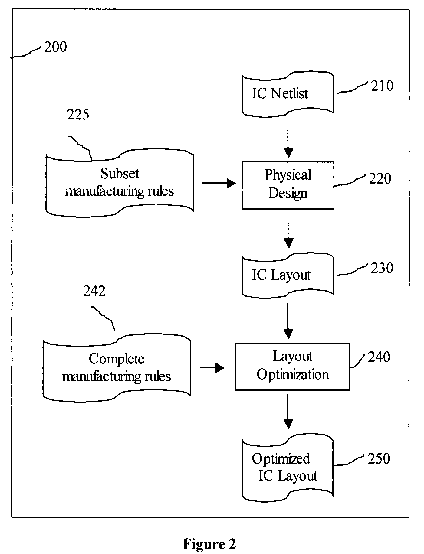
System and method to generate an IC layout using simplified manufacturing rule
a manufacturing rule and simplified technology, applied in the field of can solve the problems of inability to generate an ic layout, inability to achieve the successful generation of an ic layout, and difficult process sequence of pd procedures, so as to increase the probability of pd process successfully generating an ic layout and reduce the layout area
- Summary
- Abstract
- Description
- Claims
- Application Information
AI Technical Summary
Benefits of technology
Problems solved by technology
Method used
Image

Examples
Embodiment Construction
[0021]In the following description, numerous details are set forth for purpose of explanation. However, one of skill in the art will realize that the invention may be practiced with variations of these specific details. In other instances, well-known structures or operations are not shown in detail to avoid obscuring the invention.
Computing Environment
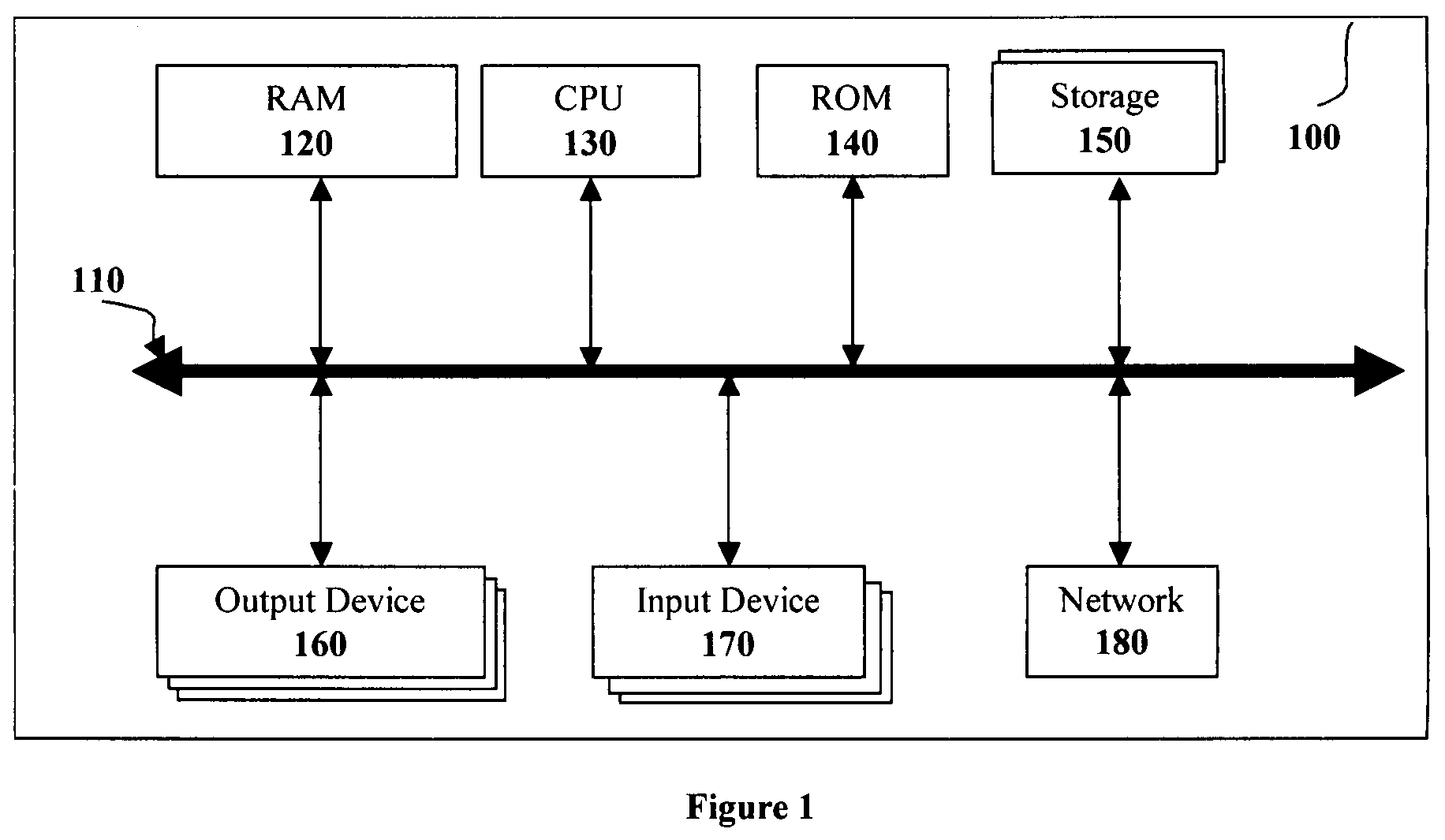
[0022]FIG. 1 illustrates a block diagram of the computing environment that one embodiment of the present invention is implemented. Even though the computer system is described with specific components and architecture for illustration, it should be understood that the present invention might be implemented in several other types of embodiments. For example, the invention can be implemented on single computer with a processor chip containing 2 or more processor cores with each core containing additional hardware to maintain state of two or more threads of execution. In addition, each component can be implemented as a combination of one ...
PUM
 Abstract
Description
Claims
Application Information