Pixel structure and active device array substrate

a technology of active devices and array substrates, applied in semiconductor devices, radio frequency controlled devices, instruments, etc., can solve problems such as degrading display quality, and achieve the effect of preventing flickering phenomenon of display frames

Active Publication Date: 2010-07-27
WUHAN CHINA STAR OPTOELECTRONICS TECH CO LTD
View PDF7 Cites 2 Cited by
  • Summary
  • Abstract
  • Description
  • Claims
  • Application Information

AI Technical Summary

Benefits of technology

[0009]The present invention is directed to provide a pixel structure capable of efficiently preventing a display frame flicker phenomenon.
[0010]The present invention is also directed to provide an active device array substrate, which enables the pixels to have a similar feedthrough voltage, so as to improve the display quality.
[0018]In an embodiment of the present invention, the scan line may transmit a switch signal to the pixel structure, and the area of the patterned semiconductor layer in the pixel structure is gradually increased in the transmission direction of the switch signal.
[0022]The capacitance of the storage capacitor of the present invention may be adjusted by changing a size of the area of the patterned semiconductor layer. Therefore, the pixel structures at the different positions of the active device array substrate of the present invention may have a consistent feedthrough voltage. As such, the active device array substrate of the present invention may efficiently prevent a display frame flicker phenomenon, thereby improving the display quality.

Problems solved by technology

In this manner, the difference between the feedthrough voltages ΔVp1 and ΔVp2 may possibly cause an effect of flicker in display frame, which degrades display quality.

Method used


Image

  • Pixel structure and active device array substrate
  • Pixel structure and active device array substrate
  • Pixel structure and active device array substrate

Examples


Embodiment Construction

[0031]Reference will now be made in detail to the present preferred embodiments of the invention, examples of which are illustrated in the accompanying drawings. Wherever possible, the same reference numbers are used in the drawings and the description to refer to the same or like parts.

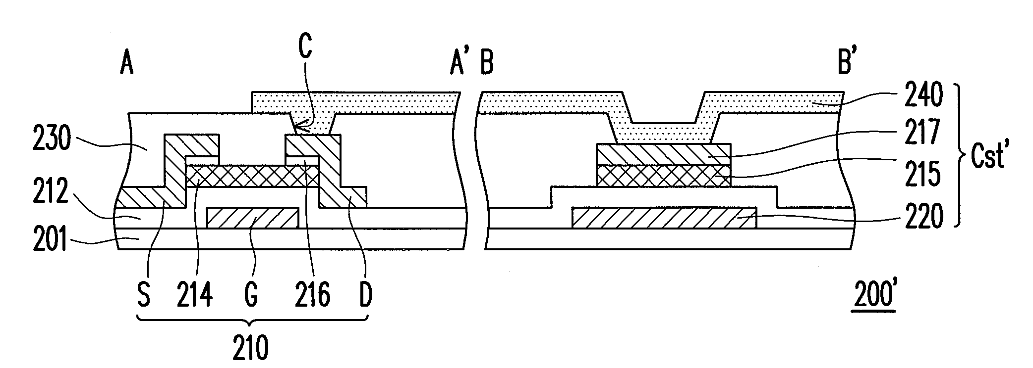
[0032]FIG. 2A is a schematic view of an active device array substrate according to an embodiment of the present invention, and FIG. 2B is a schematic sectional view of a pixel structure taken along sectional lines A-A′ and B-B′ according to an embodiment of the present invention. Referring to FIGS. 2A and 2B, the active device array substrate 300 of the present invention includes a substrate 201 and a plurality of pixel structures 200. The pixel structures 200 are disposed on the substrate 201 and arranged in array, and each pixel structure 200 is electrically connected to a corresponding scan line 202 and a corresponding data line 203. In detail, the scan line 202 may transmit a switch signal to seq...


PUM


Abstract

A pixel structure including an active device, a common line pattern, a protective layer, a pixel electrode, and a patterned semiconductor layer is provided. The active device is disposed on a substrate. In addition, the common line pattern is disposed on the substrate and covered with an insulation layer. The protective layer covers the active device and a part of the insulation layer. The protective layer has a contact window exposing the active device. The pixel electrode is disposed on the protective layer and electrically connected to the active device through the contact window. The patterned semiconductor layer is disposed on the insulation layer above the common line pattern. The patterned semiconductor layer is located between the common line pattern and the pixel electrode.

Description

CROSS-REFERENCE TO RELATED APPLICATION[0001]This application claims the priority benefit of Taiwan application serial no. 97100875, filed on Jan. 9, 2008. The entirety of the above-mentioned patent application is hereby incorporated by reference herein and made a part of specification.BACKGROUND OF THE INVENTION[0002]1. Field of the Invention[0003]The present invention relates to a pixel structure and an active device array substrate, and more particularly to a pixel structure and an active device array substrate capable of improving display quality.[0004]2. Description of Related Art[0005]Recently, the advancement of semiconductor devices and display devices flourishingly spreads the development of the multi-media technology. In respect of displays, thin-film transistor liquid-crystal displays (TFT-LCD) having superior features, such as high definition, compressed space occupation, low power consumption, and free of radiation gradually becomes the mainstream product in the market. ...

Claims


Application Information

Patent Timeline
Patent Type & Authority Patents(United States)
IPC IPC(8): H01L27/14
CPCH01L27/1255G02F1/136213
Inventor CHANG, YUAN-HAOCHIANG, CHIA-MING
Owner WUHAN CHINA STAR OPTOELECTRONICS TECH CO LTD
Why Eureka
Try Eureka