Contactor, contact structure provided with contactors, probe card, test apparatus, method of production of contact structure, and production apparatus of contact structure

a technology of contactors and contact structures, which is applied in the direction of semiconductor/solid-state device testing/measurement, instruments, and individual semiconductor devices. it can solve the problems of silicon finger contactor front end sticking out from the pads, deformation or damage,

Inactive Publication Date: 2010-07-27
ADVANTEST CORP
View PDF18 Cites 8 Cited by
  • Summary
  • Abstract
  • Description
  • Claims
  • Application Information

AI Technical Summary

Benefits of technology

[0010]An object of the present invention is to provide a contactor, a contact structure provided with the contactors, a probe card, a test apparatus, a method of production of a contact structure, and a production apparatus of a contact structure able to prevent mistaken contact with contacts.

Problems solved by technology

At the time of contact of the silicon finger contactors and pads, variations of the silicon finger contactors in the height direction cause certain silicon finger contactors on the probe board to contact the pads of the ICs first, then the first contacting silicon finger contactors are excessively overdriven until all of the silicon finger contactors provided on the probe board contact the pads of the ICs.
For that reason, for example, if the size of the pads of the ICs become small, the front ends of the silicon finger contactors end up sticking out from the pads or deforming or becoming damaged.

Method used


Image

  • Contactor, contact structure provided with contactors, probe card, test apparatus, method of production of contact structure, and production apparatus of contact structure
  • Contactor, contact structure provided with contactors, probe card, test apparatus, method of production of contact structure, and production apparatus of contact structure
  • Contactor, contact structure provided with contactors, probe card, test apparatus, method of production of contact structure, and production apparatus of contact structure

Examples


first embodiment

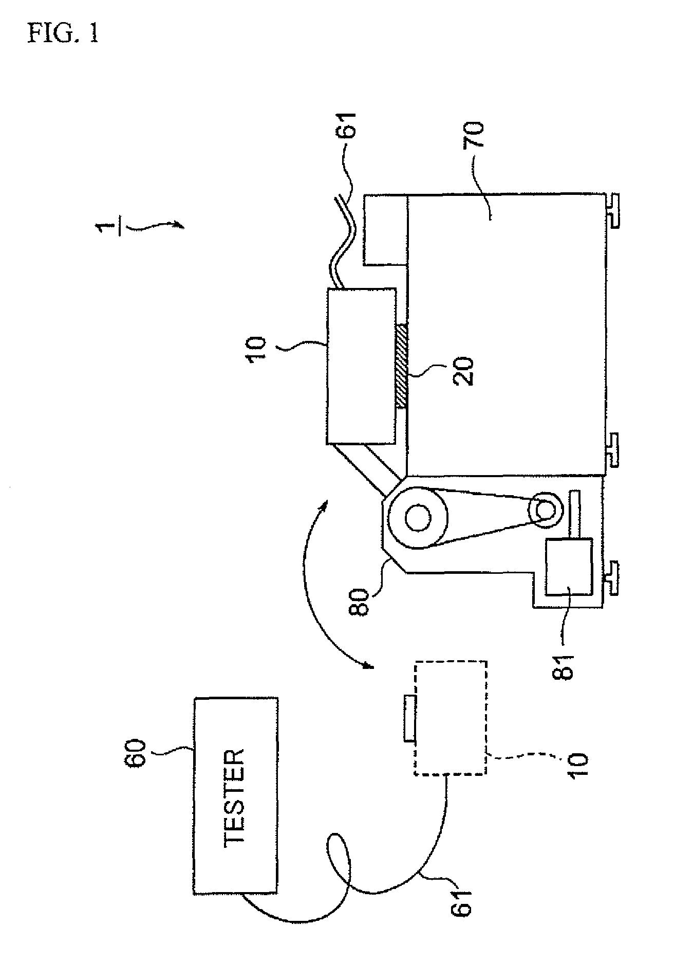
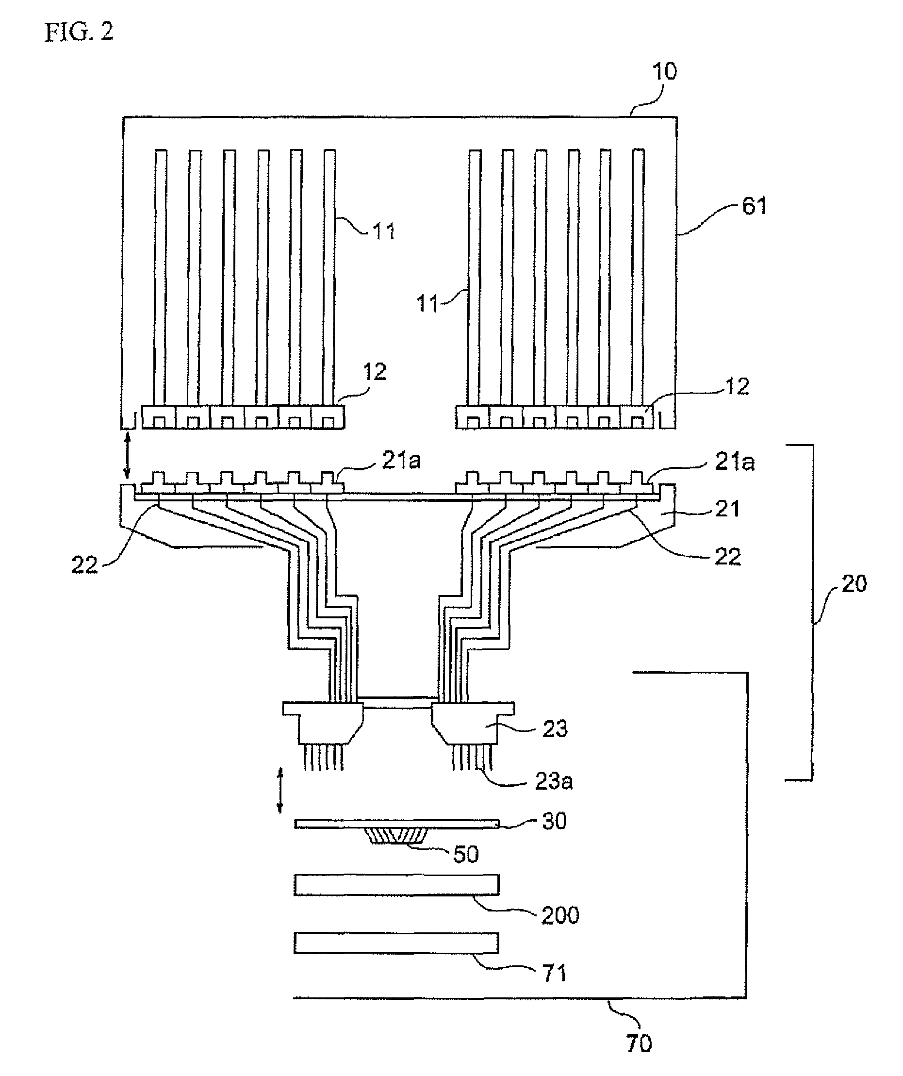
[0088]FIG. 1 is a schematic view of a test apparatus according to the present invention; while FIG. 2 is a conceptual view of the connection relationship of a test head and probe card used in the test apparatus of FIG. 1.

[0089]The test apparatus 1 according to the present embodiment, as shown in FIG. 1, is provided with a tester 60 (test apparatus body) having a test head 10 and a wafer prober 70. The test head 10 is connected through a cable bundle 61 to the tester 60. The test head 10 and wafer prober 70 are, for example, mechanically positioned and mechanically and electrically connected by a manipulator 80 and drive motor 81. The tested semiconductor wafer 200 is automatically fed by the wafer prober 70 to a test position on the test head 10.

[0090]On the test head 10, the tested semiconductor wafer 200 receives a test signal issued by the tester 60. Further, an output signal with respect to that test signal is sent from each IC of the tested semiconductor wafer 200 to the tester...

second embodiment

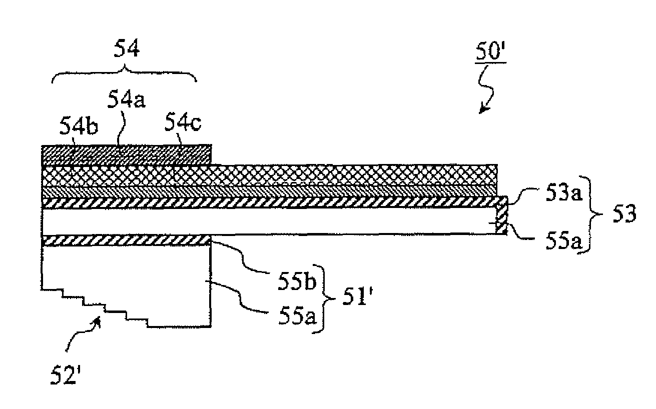
[0131]FIG. 9 is a cross-sectional view of a silicon finger contactor in the present invention.

[0132]The silicon finger contactor 50′ in the second embodiment of the present invention is formed with a plurality of the step differences 52′ in a staircase shape. Due to this, the support points of the silicon finger contactors 50 mounted on the probe board 40 increase, so the stability of attachment of the silicon finger contactor 50 with respect to the probe board 40 is improved.

[0133]Below, one example of the method of production of the probe card 30 according to the present embodiment will be explained.

[0134]FIG. 10 to FIG. 30 are views of steps for producing a silicon finger contactor in the first embodiment of the present invention, while FIG. 31A to FIG. 31C are plan views showing a silicon wafer for simultaneously producing a large number of silicon finger contactors in the first embodiment of the present invention and their cutting positions.

[0135]In the present embodiment, phot...

third embodiment

[0155]FIG. 32 is across-sectional view of a silicon finger contactor in the present invention.

[0156]The silicon finger contactor 50″ of the third embodiment of the present invention is basically comprised of a three-layer SOI wafer having three Si layers 55a and two SiO2 layers 55b sandwiched between the three Si layers.

[0157]In the present embodiment, when forming the step difference 52 of the base part 51″, instead of controlling the etching time, it is possible to use the bottom SiO2 layer 55b of the SOI wafer as an etching stopper to set the depth H of the step difference 52 to a high precision.

[0158]Note that in the present embodiment, in the etching of the Si layer 55a from the bottom surface of the SOI wafer for forming the support parts 53, the bottom SiO2 layer 55b of the SOI wafer must be removed.

[0159]Below, a production apparatus for a probe card according to an embodiment of the present invention will be explained.

[0160]FIG. 33 is a schematic view of the overall configu...


PUM


Abstract

A probe card having a plurality of silicon finger contactors contacting pads provided on a tested semiconductor wafer and a probe board mounting the plurality of silicon finger contactors on its surface, wherein each silicon finger contactor has a base part on which a step difference is formed, a support part with a rear end side provided at the base part and with a front end side sticking out from the base part, and a conductive part formed on the surface of the support part, each silicon finger contactor mounted on the probe board so that an angle part of the step difference formed on the base part contacts the surface of the probe board.

Description

BACKGROUND OF THE INVENTION[0001]1. Field of the Invention[0002]The present invention relates to a contactor, a contact structure provided with contactors, a probe card, a test apparatus, a method of production of a contact structure, and a production apparatus of a contact structure for contacting pads, electrodes, leads, or other contacts provided on an integrated circuit or other electrical circuit (hereinafter also referred to representatively as an “IC”) formed on a IC semiconductor wafer, semiconductor chip, semiconductor device package, printed circuit board, etc. to establish electric contact with the ICs when testing the ICs.[0003]2. Description of the Related Art[0004]A large number of semiconductor integrated circuit chips are formed on a silicon wafer etc., then are diced, wire bonded, packaged, and otherwise processed to produce finished electronic devices. These ICs are all tested for operation before shipment. This IC testis performed both in the finished product stat...

Claims


Application Information

Patent Timeline
Patent Type & Authority Patents(United States)
IPC IPC(8): H01H67/02
CPCG01R1/07342G01R1/07378G01R3/00H01L2924/0002H01L2924/00H01L22/00
Inventor KUITANI, TETSUYASAITO, TADAOABE, YOSHIHIRO
Owner ADVANTEST CORP
Why Eureka
Try Eureka