
Semiconductor memory device for generating back-BIAS voltage with variable driving force

a memory device and bias voltage technology, applied in the field of semiconductor memory devices for generating back bias voltage with variable driving force, can solve the problems of reducing the refresh period of the semiconductor memory device, coupling effect, and unstable operation of the cell transistor, so as to achieve constant refresh period and reduce current consumption

Active Publication Date: 2010-08-03
SK HYNIX INC
View PDF11 Cites 2 Cited by
  • Summary
  • Abstract
  • Description
  • Claims
  • Application Information

AI Technical Summary

Benefits of technology

[0032]Accordingly, current consumption can be reduced at the standby mode of the semiconductor memory device and the back-bias voltage VBB can be produced with a stable voltage level at the active mode of the semiconductor memory device regardless of the voltage level fluctuation of a boosted voltage VPP. Further, the semiconductor memory device can have a constant period of refresh.

Problems solved by technology

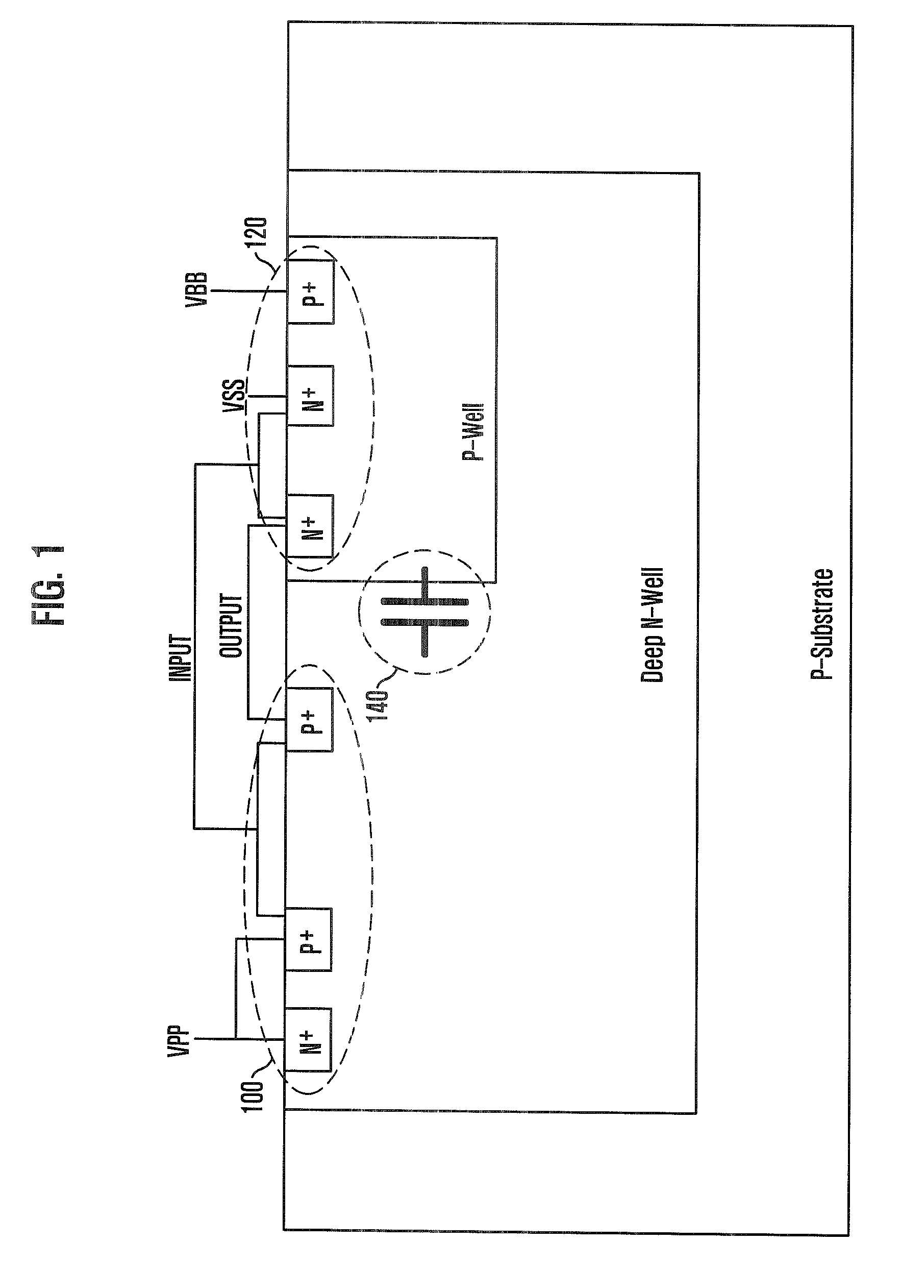
However, the coupling effect can be caused by parasitic capacitance between the back bias voltage and the boosted voltage because of the structure of MOS transistors which are employed in a peripheral circuit such as a word line control circuit.
The fluctuation in the voltage level of the back-bias voltage, which is dependent upon the operation modes of the semiconductor memory device, causes the increase of the channel leakage current in a memory cell of the semiconductor memory device and also causes an unstable operation of a cell transistor.
As a result, these shortages decrease the period of refresh in the semiconductor memory device.

Method used


Image

  • Semiconductor memory device for generating back-BIAS voltage with variable driving force
  • Semiconductor memory device for generating back-BIAS voltage with variable driving force
  • Semiconductor memory device for generating back-BIAS voltage with variable driving force

Examples


Embodiment Construction

[0037]Hereinafter, the present invention will be described in detail through embodiments with reference to the accompanying drawings.

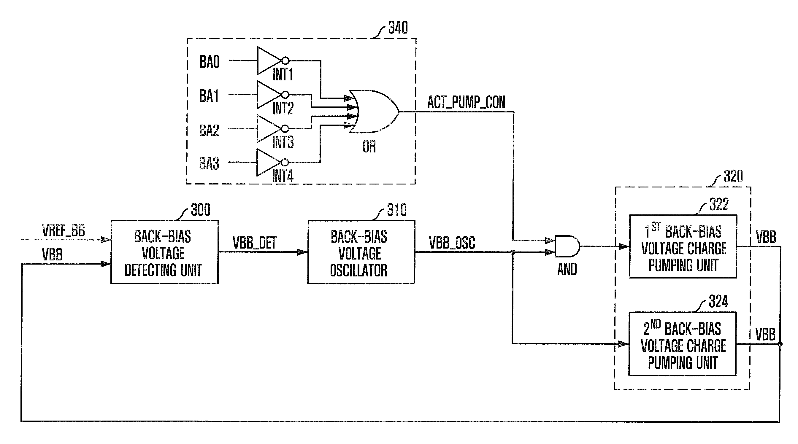
[0038]FIG. 3 is a block diagram illustrating a back-bias voltage generating circuit in accordance with an embodiment of the invention.

[0039]Referring to FIG. 3, the back-bias voltage generating circuit includes an active pumping control signal generating unit 340, a back-bias voltage detecting unit 300, a back-bias voltage oscillator 310, and a charge pumping unit 320. The active pumping control signal generating unit 340 generates an active pumping control signal ACT_PUMP_CON in response to a plurality of active signals BA0, BA1, BA2 and BA3. The back-bias voltage detecting unit 300 detects a voltage level of a back-bias voltage VBB. The back-bias voltage oscillator 310 generates an oscillation signal VBB_OSC oscillating at a predetermined frequency in response to a back-bias detection signal VBB_DET of the back-bias voltage detecting unit 300. The ch...


PUM


Abstract

A semiconductor memory device is capable of maintaining a predetermined back-bias voltage level regardless of operation modes of the semiconductor memory device, by generating a back-bias voltage with driving force changed according to the operation modes. The semiconductor memory device includes an active pumping control signal generating unit for generating an active pumping control signal in response to a plurality of active signals, a voltage detecting unit for detecting a voltage level of a back-bias voltage terminal to output a detection signal, an oscillator for generating an oscillation signal oscillating at a predetermined frequency in response to the detection signal, and a charge pumping unit for performing a charge pumping operation in response to the oscillation signal by controlling a force of driving the back-bias voltage terminal in response to the active pumping control signal.

Description

CROSS-REFERENCE TO RELATED APPLICATION[0001]The present application claims priority to Korean application number 10-2007-0138582, filed on Dec. 27, 2007, which is incorporated by reference in its entirety.BACKGROUND OF THE INVENTION[0002]The present invention relates to a semiconductor design technology, and more particularly to a back-bias voltage generating circuit of the semiconductor memory device. The back-bias voltage generating circuit is capable of generating a back-bias voltage with variable driving force corresponding to operation modes of the semiconductor memory device.[0003]Most semiconductor devices headed by DRAMs are provided with an internal voltage generator in a chip to generate a plurality of internal voltages for themselves. The plurality of internal voltages, which are required to operate internal circuits in the chip, are generated to a plurality of voltage levels by using a power supply voltage VDD and a ground voltage VSS from an external circuit.[0004]Gener...

Claims


Application Information

Patent Timeline
Patent Type & Authority Patents(United States)
IPC IPC(8): G11C7/00
CPCG11C5/145G11C11/4074
Inventor PARK, JAE-BOUM
Owner SK HYNIX INC
Learn More