Method for depositing titanium nitride films for semiconductor manufacturing

a technology of titanium nitride and semiconductors, applied in the field of semiconductor processing, can solve the problems of deteriorating the electronic characteristics of the semiconductor device, poor step coverage, and low growth rate of tin compared to cvd methods, and achieves good step coverage, good film quality, and high deposition rate of conformal tin films.

Active Publication Date: 2010-08-17
TOKYO ELECTRON LTD
View PDF18 Cites 58 Cited by
  • Summary
  • Abstract
  • Description
  • Claims
  • Application Information

AI Technical Summary

Problems solved by technology

These deposition methods suffered from poor step coverage over high-aspect ratio features found in advanced semiconductor devices, thereby requiring development of new deposition methods able to provide conformal deposition of thin TiN films that must be as thin as possible to accommodate the higher aspect ratios of today's devices.
Reaction byproducts from the CVD process include chlorine that may diffuse into the semiconductor substrate and deteriorate the electronic characteristics of the semiconductor device.
One drawback of ALD is that the growth rate for TiN can be very low compared to CVD methods.
Although these new CVD and ALD processes provide important temperature improvements over chlorine-based processes, they suffer from a variety of problems that make these processes unsatisfactory for advanced semiconductor manufacturing where film conformality, high step coverage over high-aspect ratio structures, and high deposition rate for high volume throughput are required.

Method used


Image

  • Method for depositing titanium nitride films for semiconductor manufacturing
  • Method for depositing titanium nitride films for semiconductor manufacturing
  • Method for depositing titanium nitride films for semiconductor manufacturing

Examples


Embodiment Construction

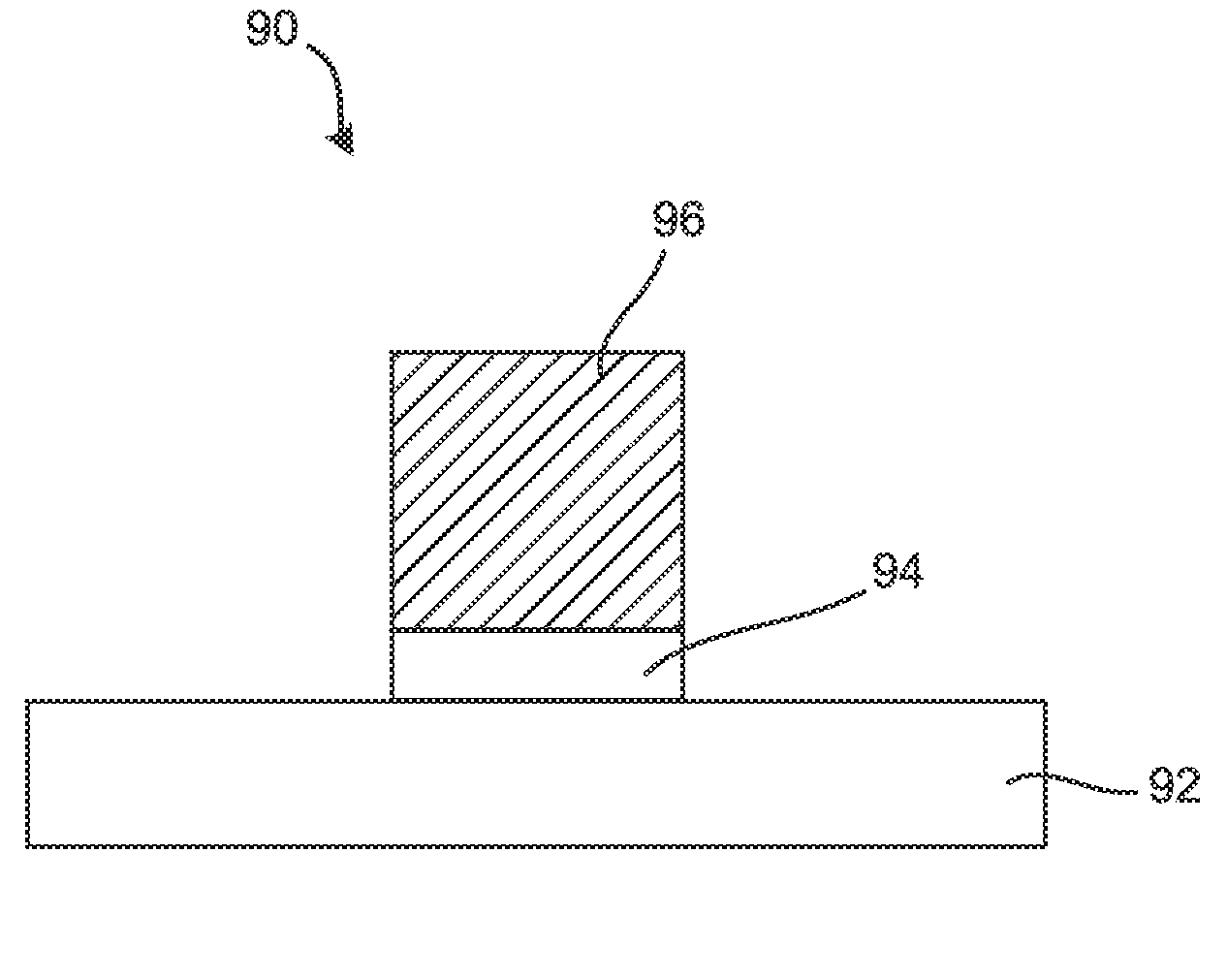
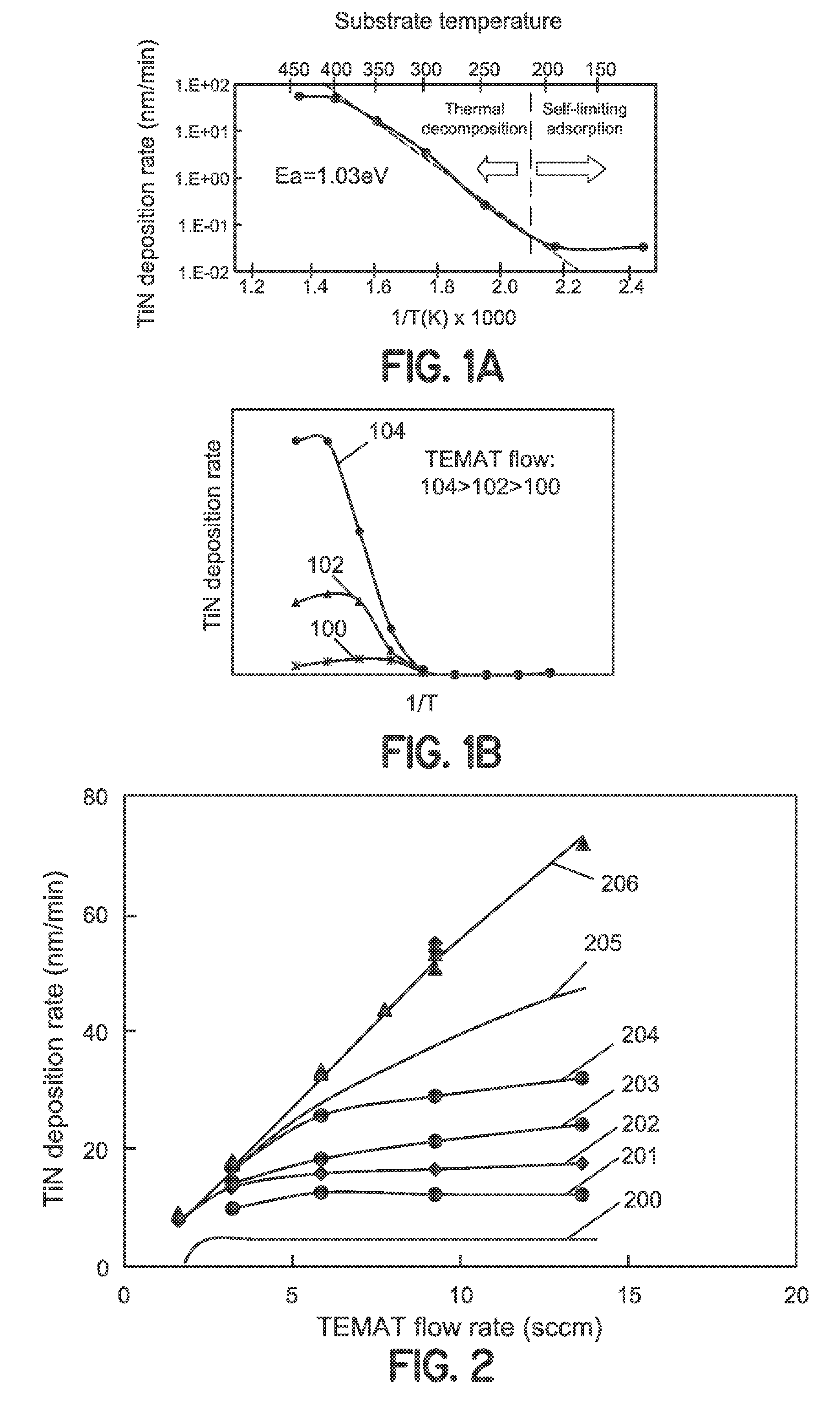
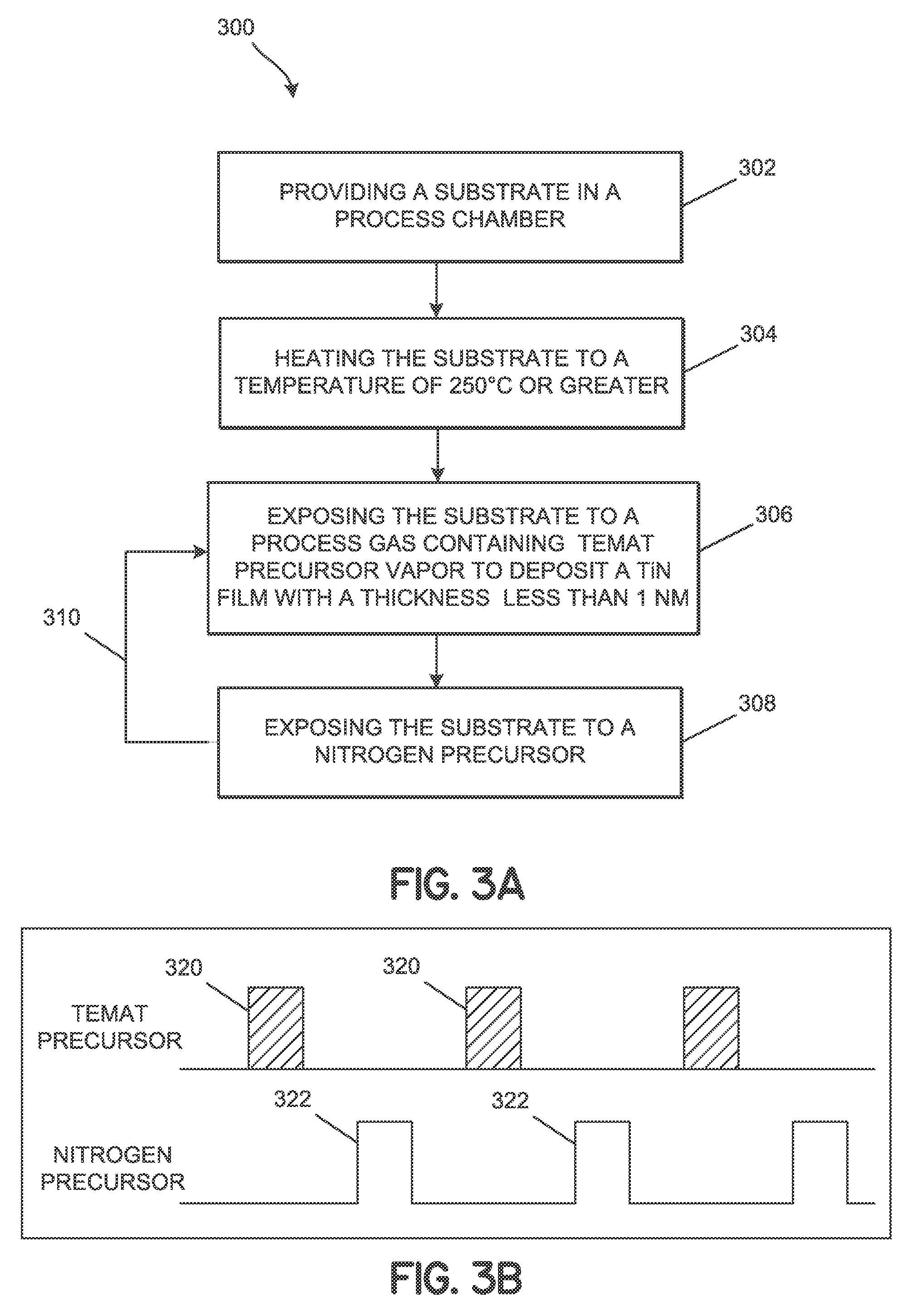
[0021]Embodiments of the invention describe processing methods that are suitable for deposition of TiN films for high volume manufacturing of semiconductor devices on large patterned substrates such as 200 mm, 300 mm, or even larger diameter substrates (wafers). The TiN films contain titanium (Ti) and nitrogen (N) but may also contain impurities such as carbon (C), oxygen (O) and hydrogen (H), that may become incorporated into the TiN films during deposition or during substrate transfer and exposure to an oxygen-containing environment such as air. In one example, the amount of C in the TiN films may be similar to or greater than that of Ti and N. In another example, the amounts of Ti, N, C, and O in air exposed TiN films may be similar.

[0022]According to embodiments of the invention, a titanium amide precursor, tetrakis(ethylmethylamino) titanium (TEMAT), is utilized for conformal TiN film deposition. TEMAT (Ti(N(CH3)C2H5)4) has a molecular weight of 280.32 g / mol, density of 0.95 g / ...


PUM

PropertyMeasurementUnit
temperatureaaaaaaaaaa
thicknessaaaaaaaaaa
thicknessaaaaaaaaaa

Abstract

Embodiments of the invention describe TiN deposition methods suitable for high volume manufacturing of semiconductor devices on large patterned substrates (wafers). One embodiment describes a chemical vapor deposition (CVD) process using high gas flow rate of a tetrakis(ethylmethylamino) titanium (TEMAT) precursor vapor along with an inert carrier gas at a low process chamber pressure that provides high deposition rate of conformal TiN films with good step coverage in surface reaction limited regime. Other embodiments describe cyclical TiN deposition methods using TEMAT precursor vapor and a nitrogen precursor.

Description

CROSS-REFERENCE TO RELATED APPLICATIONS[0001]This application is related to U.S. patent application Ser. No. 11 / 743,548,entitled “METHOD FOR DEPOSITING TITANIUM NITRIDE FILMS FOR SEMICONDUCTOR MANUFACTURING,” filed on even date herewith, the entire content of which is hereby incorporated by reference.FIELD OF THE INVENTION[0002]The present invention relates to semiconductor processing, and more particularly to chemical vapor deposition and cyclical deposition methods suitable for high volume manufacturing of titanium nitride (TiN) films in semiconductor devices.BACKGROUND OF THE INVENTION[0003]Titanium nitride (TiN) films are widely used in semiconductor devices and ultra-large-scale integrated circuits. For example, TiN films have been used in semiconductor devices as a diffusion barrier for preventing metal diffusion into other materials. TiN films have been employed as a diffusion barrier against copper (Cu) diffusion, for example in contacts, vias and trenches. Other uses includ...

Claims


Application Information

Patent Timeline
Patent Type & Authority Patents(United States)
IPC IPC(8): H01L21/44
CPCC23C16/34C23C16/45527H01L21/28562
Inventor HASEGAWA, TOSHIO
Owner TOKYO ELECTRON LTD
Why Eureka
Try Eureka