Energy transfer device and energy transfer control semiconductor device

a technology of energy transfer device and semiconductor device, which is applied in the direction of dc-dc conversion, power conversion system, instruments, etc., can solve the problems of difficult effective suppression of switching noise, malfunction and failure, and adverse effects on other electronic devices, so as to reduce the size and cost of the device

Active Publication Date: 2010-08-17
PANASONIC SEMICON SOLUTIONS CO LTD
View PDF10 Cites 48 Cited by
  • Summary
  • Abstract
  • Description
  • Claims
  • Application Information

AI Technical Summary

Benefits of technology

[0038]The present invention is made to solve the conventional problems described above, and an object thereof is to provide an energy transfer device and an energy transfer control semiconductor device capable of reducing switching noise associated with a switching operation using a simple and small component configuration in an RCC-type switching power supply including pseudo-resonance control and the like, limiting cost increase, and particularly during high voltage input under a W / W (worldwide) AC input specification or voltage input under a DC input specification, effectively reducing an average value of a noise terminal voltage that leaks outward from a commercial power supply that supplies such input voltage.

Problems solved by technology

However, the switching power supply generates high levels of switching noise while performing switching operations by turning on / off a switching element, and therefore may potentially have adverse effects on other electronic devices such as malfunction and failure.
However, in many cases, effectively suppressing switching noise is difficult and requires a large number of noise suppression parts.
Consequently, power supply costs and area increase, and considerable effort ends up being spent on measures against noise.
However, since a conventional switching power supply as disclosed in Japanese Patent Laid-Open No. 2005-295637 employs a PWM control method that is a hard switching method, while diffusing the switching frequency reduces the average value of the noise terminal voltage, the Qp value remains high.
However, the switching frequency variable circuit for diffusing frequency requires more parts, resulting in an increase in power supply cost even though the effort spent on measures against switching noise is reduced.
However, input ripple voltage during high input is low and the variation in oscillating frequency is significantly small.
However, during high input, since the diffusion of oscillating frequency due to input ripple voltage is small, the noise average value tends to deteriorate.
While the input electrolytic capacitor capacity can conceivably be reduced during high input, in order to ensure that the oscillating frequency diffuses, the reduction in the input electrolytic capacitor capacity disadvantageously increases input ripple voltage during low input significantly, which in turn shortens the life cycle of the input electrolytic capacitor.

Method used


Image

  • Energy transfer device and energy transfer control semiconductor device
  • Energy transfer device and energy transfer control semiconductor device
  • Energy transfer device and energy transfer control semiconductor device

Examples


first embodiment

[0087]An energy transfer device according to a first embodiment of the present invention will be described.

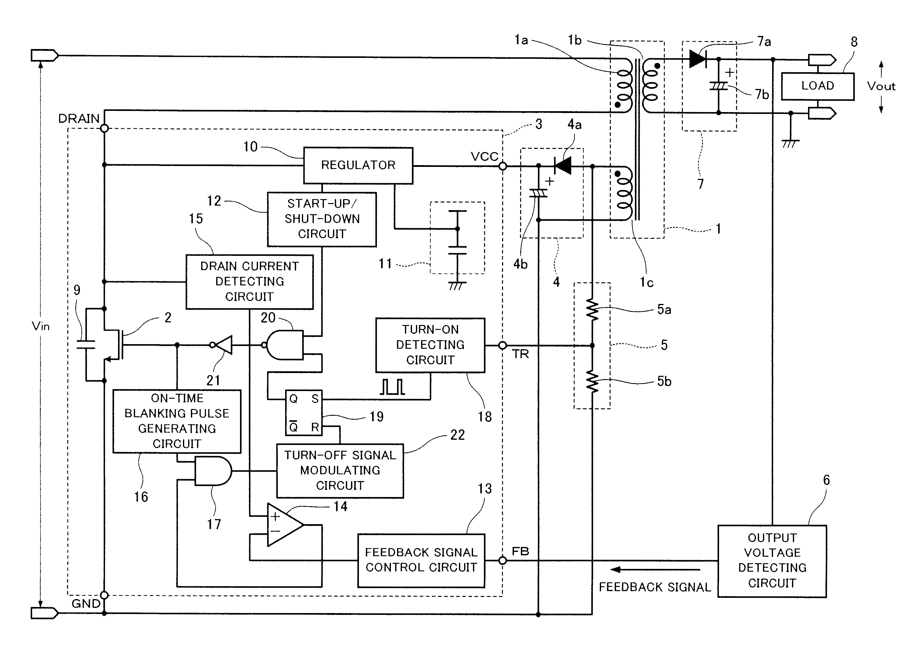
[0088]FIG. 1 is a circuit diagram showing a configuration example of the energy transfer device including an energy transfer control semiconductor device according to the present first embodiment.

[0089]In FIG. 1, a transformer 1 includes a primary winding 1a, a secondary winding 1b, and an auxiliary winding 1c. The primary winding 1a and the secondary winding 1b have reverse polarities. This energy transfer device, i.e., a switching power supply, is of a flyback type.

[0090]A switching element 2 is connected to the primary winding 1a. On / off switching control of a control electrode (gate) of the switching element 2 is performed by an output signal of a control circuit 3.

[0091]The control circuit 3 that is a semiconductor device includes the switching element 2, whereby the switching element 2 constituted by a power MOSFET or the like is integrated on the same semiconductor subst...

second embodiment

[0161]Next, an energy transfer control semiconductor device according to a second embodiment of the present invention will be described.

[0162]FIG. 7 is a circuit diagram showing a configuration example of an energy transfer device including the energy transfer control semiconductor device according to the present second embodiment. In comparison with the first embodiment, in the present second embodiment, a signal is inputted from a feedback signal control circuit 23 to a turn-off signal modulating circuit 22. A primary object of the present second embodiment is to modulate a delay time tf(t) by the turn-off signal modulating circuit 22 in accordance with a feedback signal or, in other words, depending on a load condition of an output voltage Vout.

[0163]Since a description of operations is similar to the first embodiment described above, only modifications will be described hereafter. In addition, reference numerals are omitted for elements already described in the first embodiment....

third embodiment

[0176]Next, an energy transfer control semiconductor device according to a third embodiment of the present invention will be described.

[0177]FIG. 10 is a circuit diagram showing a configuration example of an energy transfer device including the energy transfer control semiconductor device according to the present third embodiment. In comparison with the first embodiment, in the present third embodiment, a control circuit 3 has been provided with an LS terminal and a resistor 30 is inserted between an input voltage Vin and the LS terminal.

[0178]In addition, a current inputted to the LS terminal from the input Vin via the resistor 30 is to be inputted to an input voltage detecting circuit 24 and a signal in accordance with the current value is to be inputted to a turn-off signal modulating circuit 22, and a primary object of the present third embodiment is to modulate a delay time tf(t) by the turn-off signal modulating circuit 22 in accordance with the magnitude of the input voltage ...


PUM


Abstract

The present invention includes a turn-off signal modulating circuit that periodically varies a turn-off timing of a switching element 2 at a preset modulation time after a current detection by a drain current detecting circuit 15, and by modulating the peak of a current flowing through the switching element 2, diffuses switching noise while preventing concentration of an oscillating frequency at a constant frequency even under a constant input voltage and a constant load.

Description

FIELD OF THE INVENTION[0001]The present invention relates to an energy transfer device that controls an output voltage by switching an input voltage through a switching element, and an energy transfer control semiconductor device constituting the energy transfer device.BACKGROUND OF THE INVENTION[0002]Conventionally, in ordinary household equipment such as home appliances, a switching power supply including a switching power supply control semiconductor device that controls (stabilization or the like) an output voltage through a switching operation by a semiconductor (a switching element such as a transistor) has been widely used as a power supply for the purposes of improving power efficiency by reducing power consumption and the like.[0003]However, the switching power supply generates high levels of switching noise while performing switching operations by turning on / off a switching element, and therefore may potentially have adverse effects on other electronic devices such as malf...

Claims


Application Information

Patent Timeline
Patent Type & Authority Patents(United States)
IPC IPC(8): H02M3/335
CPCH02M3/33507H02M1/44
Inventor YAMASHITA, TETSUJI
Owner PANASONIC SEMICON SOLUTIONS CO LTD
Why Eureka
Try Eureka