Method of forming vertical structure light emitting diode with heat exhaustion structure

a technology of light-emitting diodes and vertical structures, which is applied in the direction of basic electric elements, electrical apparatus, and semiconductor devices

Inactive Publication Date: 2010-08-24
WALSIN LIHWA
View PDF2 Cites 25 Cited by
  • Summary
  • Abstract
  • Description
  • Claims
  • Application Information

AI Technical Summary

Benefits of technology

[0009]In accordance with an aspect of the present invention, a method of forming a vertical structure light emitting diode (LED) with heat exhaustion structure includes the steps of: a) providing a sapphire substrate; b) producing a number of recesses on the sapphire substrate, each of which has a depth of p; c) forming a buffer layer having a number of protrusions, each of which has a height of q smaller than p so that when the protrusions of the buffer layer are accommodated within the recesses of the sapphire substrate, a number of gaps are formed therebetween for heat exhaustion; d) growing a number of luminescent layers on the buffer layer, having a medium layer formed between the luminescent layers and the buffer layer; e) etching through the luminescent layers and the buffer layer to form a duct for heat exhaustion; f) removing the sapphire substrate by excimer laser lift-off (LLO); g) roughening the medium layer; and h) depositing electrodes on the roughened medium layer.

Problems solved by technology

In recent years, the heat dissipation management is still the main issue on the development for packaged high power LEDs under high current driving.
For the lateral current conducting structure epitaxied on sapphire substrate, there are drawbacks on the current crowding effect, high series resistance and poor heat dissipation.
It may be needed for laser beam to scan an epitaxial wafer more than one time, which decreases the throughput and increases the chance of damaging the epitaxial layer of LEDs.
Also, the laser lift-off equipment is expensive.
However, the thermal conductivity of the sapphire substrate is not so good that the blue light emitting diode is limited to a lateral conducting structure with its positive and negative metal electrodes on the same side of the substrate.
Thus, the structure substantially shrinks the lighting area.
Besides, due to current crowding effect and lateral path, there are inevitable increases in series resistance (Rs) and forward voltage drop (Vf) of the LED device.
The huge amount of heat generated decays external quantum efficiency directly.
Although it is commercialized, the manufacturing cost of such LED device is still quite expensive due to its complex processes and low yield.
Subsequently, the released nitrogen gas may cause damage to neighboring insolated epitaxial elements and the heat dissipation substrate due to the pressure thus formed.
Therefore, the peeling of the fragile interface formed by bonding or electroplating technology may produce the issue on reliability, for example, fast degradation of light output power, increase of forward voltage drop after package.
In order to improve the yield rate of LLO, main isolated street path between adjacent two epitaxial elements is necessarily enlarged, which causes low production in a 2-inch wafer and indirectly increases the manufacturing cost.

Method used


Image

  • Method of forming vertical structure light emitting diode with heat exhaustion structure
  • Method of forming vertical structure light emitting diode with heat exhaustion structure
  • Method of forming vertical structure light emitting diode with heat exhaustion structure

Examples


Embodiment Construction

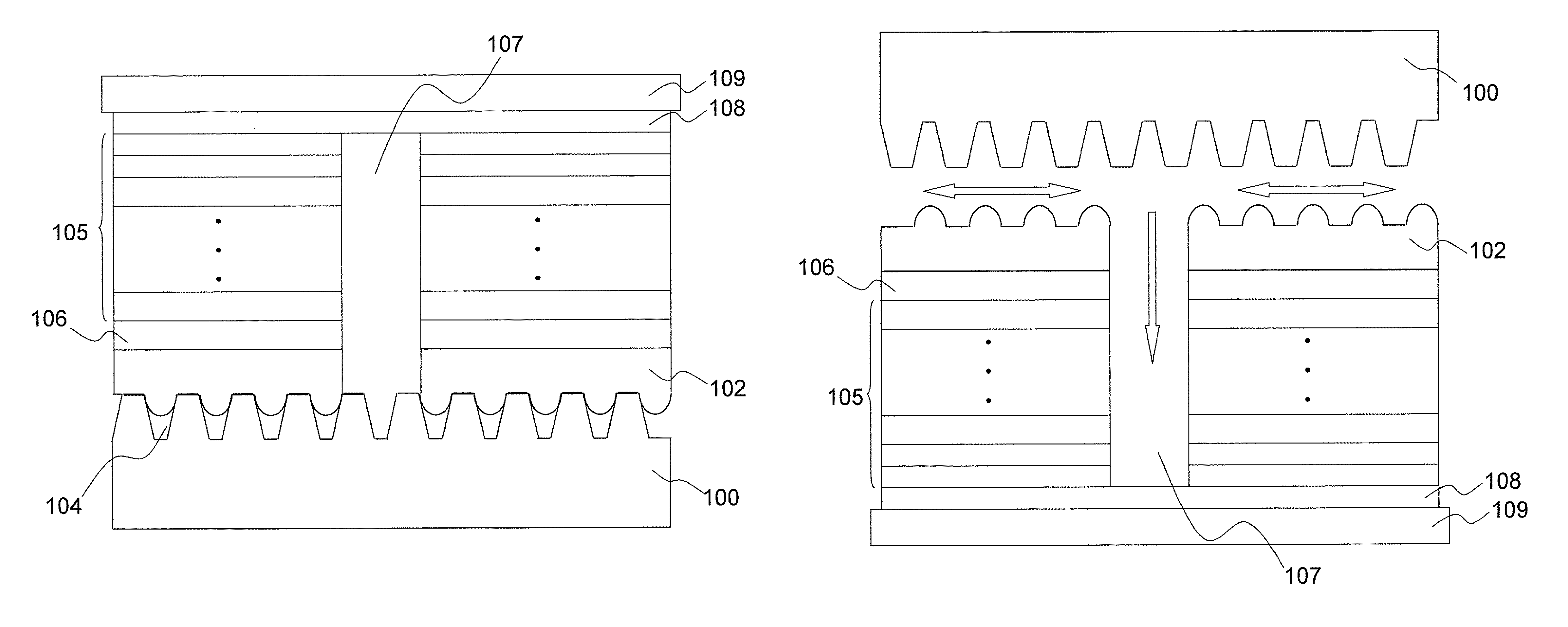
[0024]In order to exhaust heat caused by current crowding effect, a vertical structure light emitting diode with a heat exhaustion structure is desired. An embodiment of the present invention showing a method of forming a vertical structure light emitting diode with heat exhaustion structures is shown below.

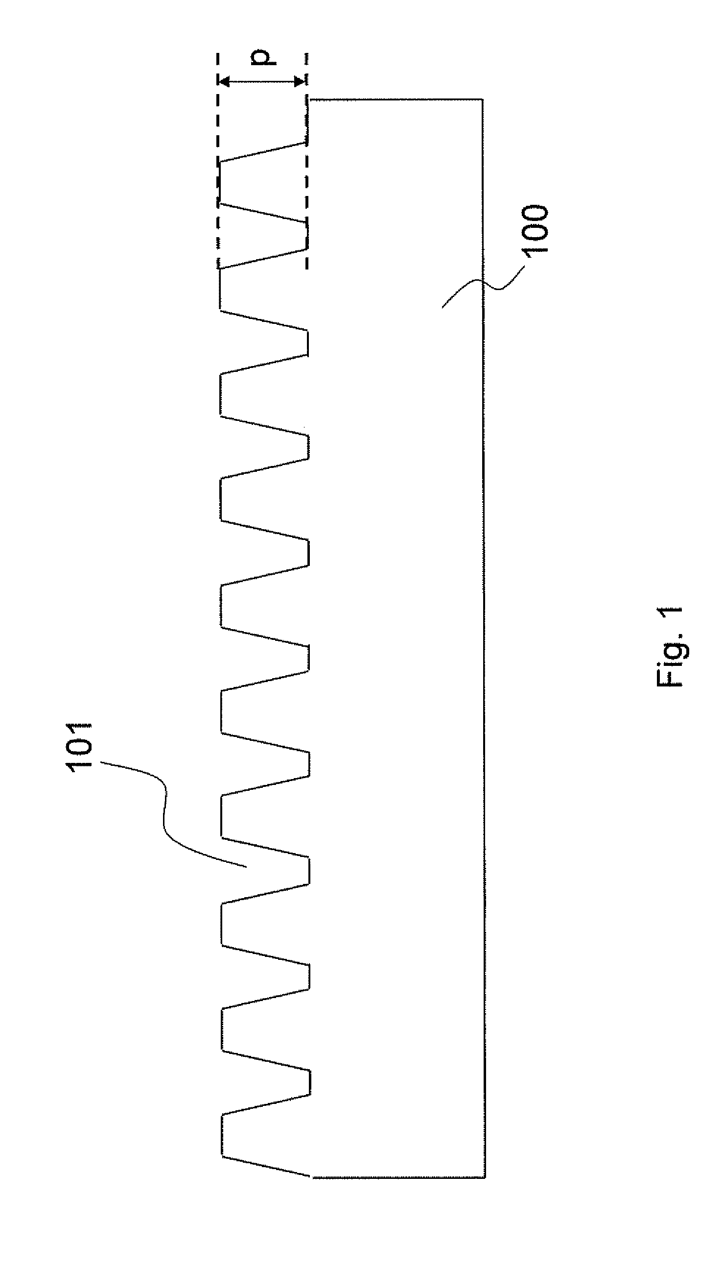
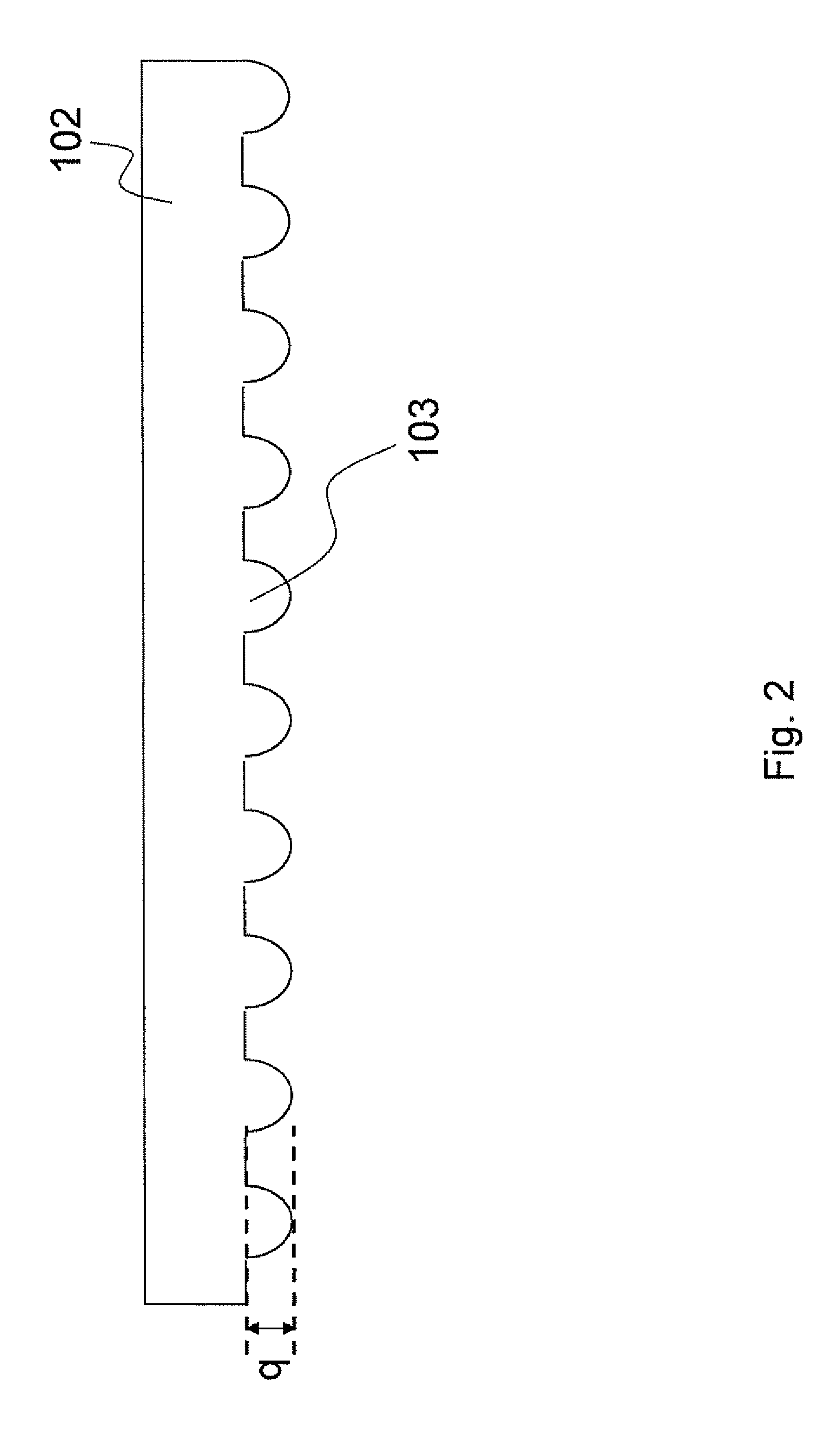
[0025]Please refer to FIGS. 1 to 9. A first embodiment is illustrated. In this embodiment, a sapphire substrate 100 is first provided. Then, a number of recesses 101 are formed on the sapphire substrate 100 by photolithographic process, wet etching process, or dry etching process. Each of the recesses 101 has a depth of p and a recess width of m. Next, a buffer layer 102 having a number of protrusions 103, each of which has a height of q and a protrusion width of n, is formed above the sapphire substrate 100.

[0026]The protrusions 103 of the buffer layer 102 are accommodated within the recesses 101 of the sapphire substrate 100. A number of gaps 104 are formed for heat exhaustion ...


PUM


Abstract

A method of forming a vertical structure light emitting diode with a heat exhaustion structure, comprising the steps of: providing a sapphire substrate; producing a number of recesses on the sapphire substrate, each of which has a depth of p; forming a buffer layer having a number of protrusions, each of which has a height of q smaller than p so that when the protrusions of the buffer layer are accommodated within the recesses of the sapphire substrate, a number of gaps are formed therebetween for heat exhaustion; growing a number of luminescent layers on the buffer layer, having a medium layer formed between the luminescent layers and the buffer layer; etching through the luminescent layers and the buffer layer to form a duct for heat exhaustion; removing the sapphire substrate by excimer laser lift-off (LLO); roughening the medium layer; and depositing electrodes on the roughened medium layer.

Description

FIELD OF THE INVENTION[0001]The present invention relates generally to a method of forming a vertical structure light emitting diode (LED). More specifically, the present invention relates to a method of forming a vertical structure light emitting diode (LED) having a duct and a number of gaps for heat exhaustion so that yield can be improved while laser lift-off (LLO) process is introduced and throughput of the LED can be raised.BACKGROUND OF THE INVENTION[0002]In recent years, the heat dissipation management is still the main issue on the development for packaged high power LEDs under high current driving. For the lateral current conducting structure epitaxied on sapphire substrate, there are drawbacks on the current crowding effect, high series resistance and poor heat dissipation.[0003]Then, the disadvantage of poor heat sink of sapphire can be resolved by other heat dissipation substrate by laser lift-off (LLO) process using a short wavelength excimer source. For example, U.S. ...

Claims


Application Information

Patent Timeline
Patent Type & Authority Patents(United States)
IPC IPC(8): H01L21/00
CPCH01L33/007H01L33/0079H01L33/12H01L33/0093
Inventor CHEN, SHIUE-LUNGFENG, JENG-KUOCHANG JEAN, CHING-HWACHEN, JANG-HO
Owner WALSIN LIHWA
Why Eureka
Try Eureka