Resputtering process for eliminating dielectric damage

a dielectric layer and etching technology, applied in vacuum evaporation coatings, semiconductor devices, coatings, etc., can solve the problems of reliability problems, insufficient coverage of via sidewalls, low uniformity of deposited layers, etc., to minimize the damage to the dielectric layer, improve the etching rate, and improve the quality of deposited layers

Inactive Publication Date: 2010-08-24
NOVELLUS SYSTEMS
View PDF171 Cites 28 Cited by
  • Summary
  • Abstract
  • Description
  • Claims
  • Application Information

AI Technical Summary

Benefits of technology

[0014]The present invention pertains to iPVD-based methods of resputtering material from the wafer surface. It significantly improves several characteristics of the resputter process used for removal and redistribution of diffusion barrier layers or conductive layers of the wafer. The invention provides process conditions which minimize the damage to the dielectric layer during resputtering. The invention allows considerable etching of the diffusion barrier material at the via bottom, while not damaging exposed dielectric elsewhere on the wafer. Specifically, it provides a solution for the dielectric microtrenching problem occurring during conventional resputter process. Furthermore, the invention increases the etch rate to deposition rate (E / D) ratio, which is desirable during resputter because it improves the effectiveness of the etch back. Still further, the etch back nonuniformity (EBNU) is greatly improved by the methods of this invention. Improvement of EBNU results in better overall reliability of the IC device. In general, this invention provides IC devices with higher reliability and decreases wafer manufacturing costs.

Problems solved by technology

The deposited layer usually has low uniformity, with over-accumulation of material in the bottom of the vias and insufficient coverage of via sidewalls.
This presents a particular problem for diffusion barrier layer formation, since continuous thin layers of barrier material are universally preferred in the industry.
Insufficient coverage of sidewalls causes reliability problems due to increased diffusion of copper into the adjacent dielectric layer.

Method used


Image

  • Resputtering process for eliminating dielectric damage
  • Resputtering process for eliminating dielectric damage
  • Resputtering process for eliminating dielectric damage

Examples


Embodiment Construction

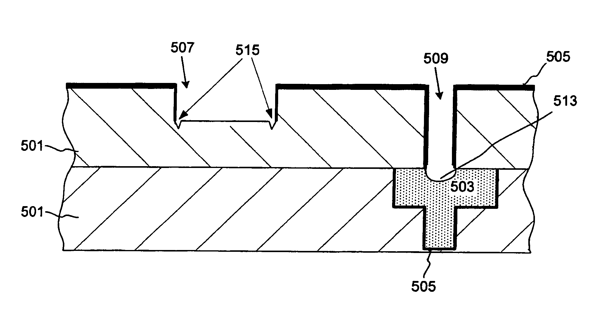
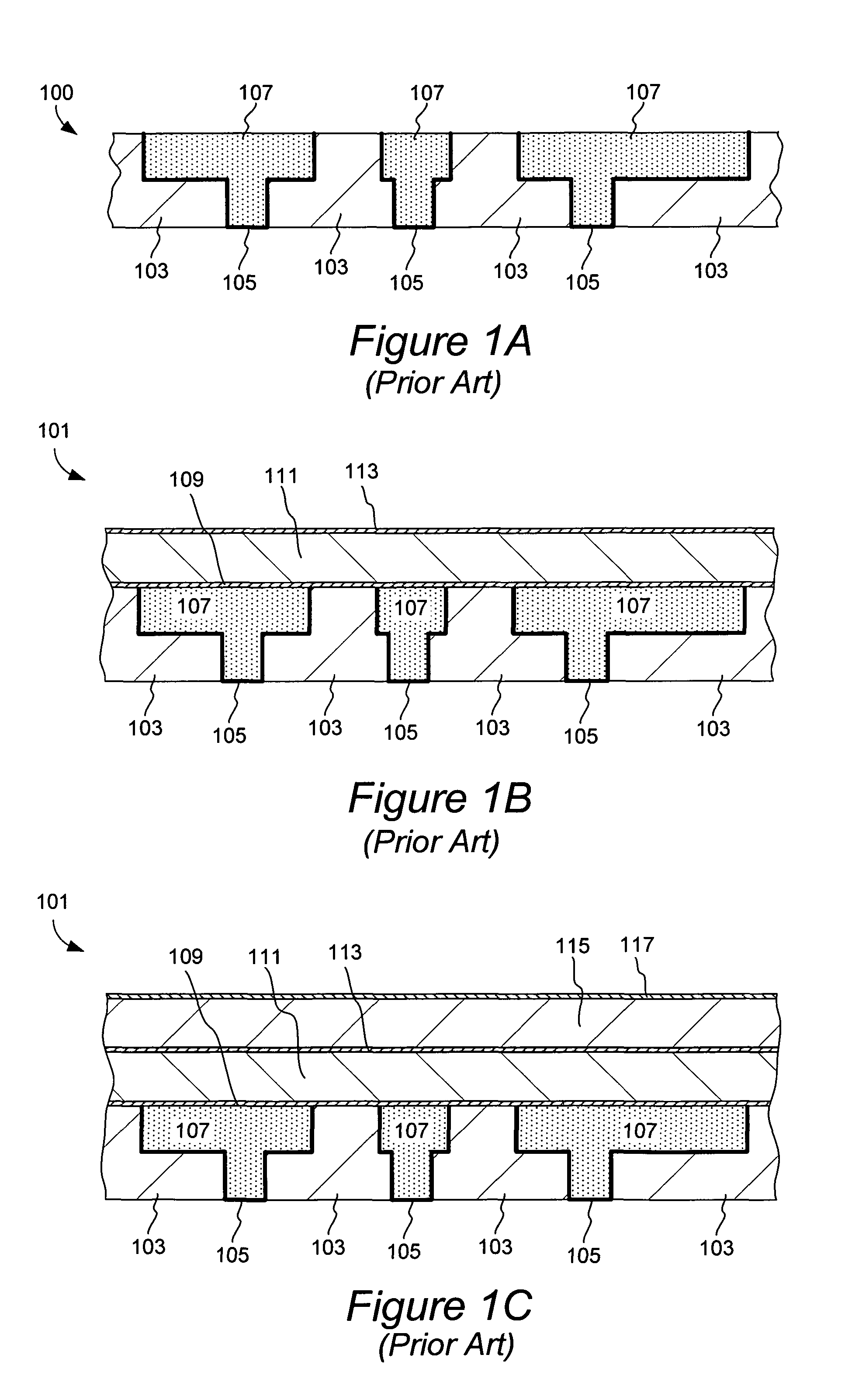
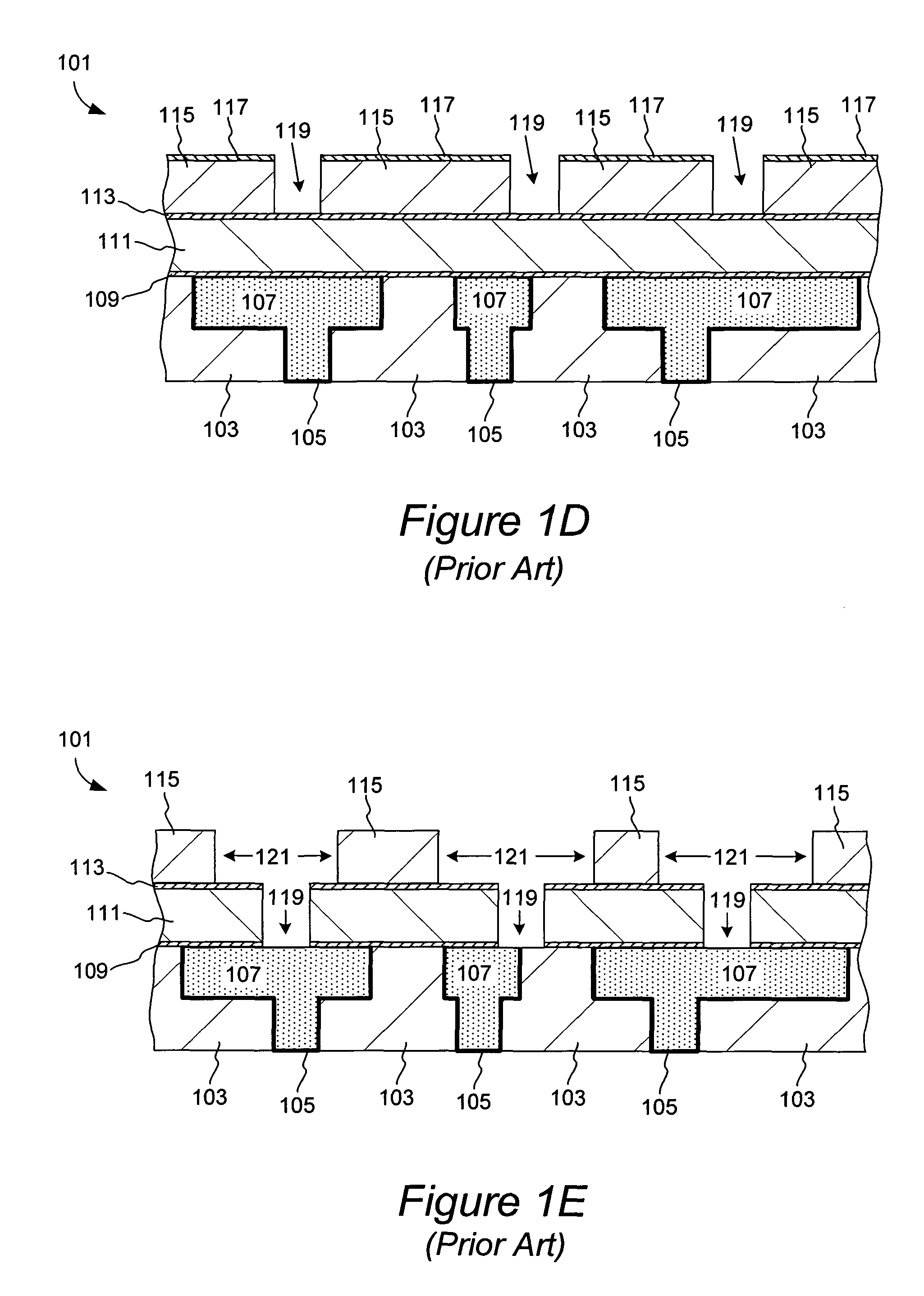
[0032]The etch-back of the barrier layer can be accomplished by a technique known as the resputter process. As explained below, resputtering may take place in the same chamber as the iPVD process and employ similar process conditions, but without significant deposition. In this process ionic species are directed towards the wafer and upon collision with the wafer surface, resputtering of the wafer material occurs. The ions are usually formed by ionization of the process gas in the iPVD magnetron chamber. However, the plasma conditions are controlled so that the gas ions do not significantly contact the target. Nevertheless, in some embodiments of this invention there may be a component of ionized metal in addition to ionized gas resputtering wafer material. Commonly employed process gases are inert gases such as argon and krypton and their mixtures with nitrogen. The resputtering process is typically carried out at temperatures of up to 500° C. The traditionally used pressure for re...


PUM

PropertyMeasurementUnit
pressureaaaaaaaaaa
pressureaaaaaaaaaa
pressureaaaaaaaaaa

Abstract

Methods of resputtering material from the wafer surface include at least one operation of resputtering material under a pressure of at least 10 mTorr. The methods can be used in conjunction with an iPVD apparatus, such as hollow cathode magnetron (HCM) or planar magnetron. The resputtered material may be a diffusion barrier material or a conductive layer material. The methods provide process conditions which minimize the damage to the dielectric layer during resputtering. The methods allow considerable etching of the diffusion barrier material at the via bottom, while not damaging exposed dielectric elsewhere on the wafer. Specifically, they provide a solution for the dielectric microtrenching problem occurring during conventional resputter process. Furthermore, the methods increase the etch rate to deposition rate ratio (E/D) and improve the etch back nonuniformity (EBNU) of resputter process. In general, the methods provide IC devices with higher reliability and decrease wafer manufacturing costs.

Description

CROSS-REFERENCE TO RELATED APPLICATIONS[0001]This application is a continuation-in-part claiming priority under 35 USC 120 from U.S. patent application Ser. No. 10 / 804,353 filed Mar. 18, 2004 (now U.S. Pat. No. 7,186,648), titled “Barrier First Method For Single Damascene Trench Applications,” naming Rozbicki et al. as inventors, which is a continuation-in-part claiming priority under 35 USC 120 from U.S. patent application Ser. No. 10 / 412,562 filed Apr. 11, 2003 (now U.S. Pat. No. 6,764,940), which is a continuation-in-part claiming priority under 35 USC 120 from U.S. patent application Ser. No. 09 / 965,472 filed Sep. 26, 2001 (now U.S. Pat. No. 6,607,977), which claims benefit of prior U.S. Provisional Application No. 60 / 275,803 filed Mar. 13, 2001. U.S. Pat. No. 6,764,940 also claims benefit of U.S. Provisional Patent Application No. 60 / 379,874 filed May 10, 2002. Each of these references is incorporated herein by reference in its entirety for all purposes.FIELD OF THE INVENTION[0...

Claims


Application Information

Patent Timeline
Patent Type & Authority Patents(United States)
IPC IPC(8): H01L21/4763
CPCH01L21/2855H01L21/76805H01L21/76814H01L21/76843H01L21/76844H01L21/76865
Inventor KAILASAM, SRIDHARROZBICKI, ROBERTYU, CHENTAOHAYDEN, DOUGLAS
Owner NOVELLUS SYSTEMS
Why Eureka
Try Eureka