Electronic apparatus

a technology of electronic equipment and components, applied in the direction of resonant antennas, electric apparatus casings/cabinets/drawers, instruments, etc., can solve the problems of increasing the cost of tim b>120/b>, the parts cannot be provided with heat-radiating components, and the inability to provide parts with heat-radiating components, etc., to achieve efficient radiation of heat generated in electronic components and improve the mounting ability of electronic equipment to the substrate

Active Publication Date: 2010-08-24
SHINKO ELECTRIC IND CO LTD
View PDF14 Cites 36 Cited by
  • Summary
  • Abstract
  • Description
  • Claims
  • Application Information

AI Technical Summary

Benefits of technology

[0011]The invention has been made in view of the above points, and the object thereof is to provide an electronic apparatus capable of reliably radiating the heat generated in an electronic element without deteriorating mountability.
[0037]According to the invention, the heat generated in the electronic element is radiated via the resin material in which the inorganic filler is mixed or the thermal via is formed in the second substrate. The thermal via is formed in the second substrate, and the mold resin is disposed between the first substrate and the second substrate. Accordingly, when the electronic apparatus is mounted onto a substrate, etc. (for example, a mother board, etc.), the thermal via or the mold resin does not affect mountability. Therefore, while the mountability of the electronic apparatus to the substrate can be improved, the heat generated in the electronic element can be efficiently radiated.

Problems solved by technology

Therefore, this part cannot be provided with the heat-radiating member.
As a result, selection of the TIM 120 is limited, and an increase in the cost of the TIM 120 is expected.
In preventing this, there is a problem in that the thickness control of the TIM 120 should be performed accurately.

Method used


Image

  • Electronic apparatus
  • Electronic apparatus
  • Electronic apparatus

Examples


first embodiment

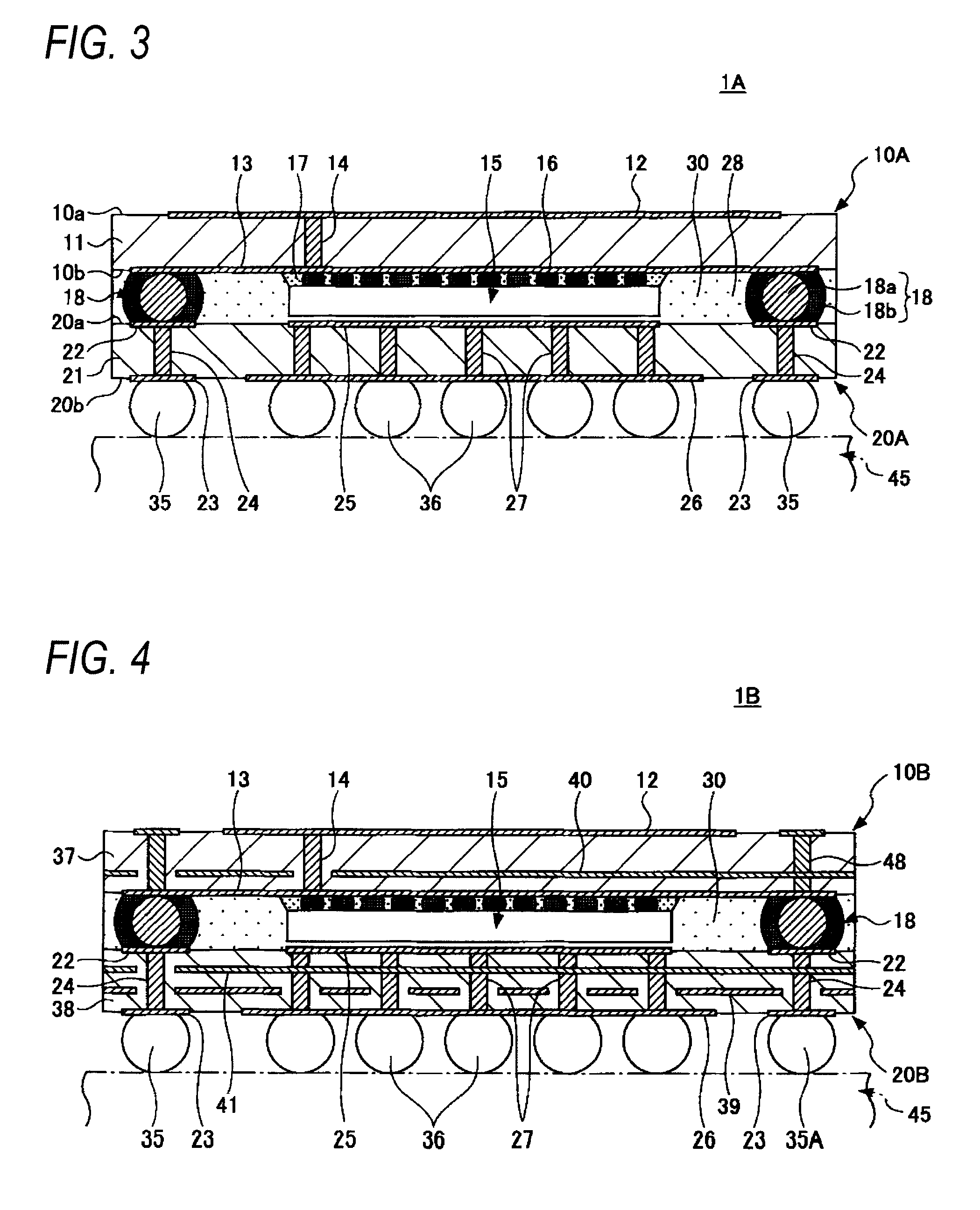
[0045]FIG. 3 is a sectional view showing an electronic apparatus 1A which is the invention. The electronic apparatus 1A has substrate structure in which an antenna 12 is formed in a surface portion, and a semiconductor chip 15 is built in. Further, the electronic apparatus 1A is mounted onto a mounting board, such as a mother board 45 (shown by one-dot chain lines in the drawing).

[0046]The electronic apparatus 1A is generally constituted by a first substrate 10A, the semiconductor chip 15, copper core solder balls 18, a second substrate 20A, a mold resin 30, etc.

[0047]The first substrate 10A is a double-sided printed circuit board, and uses a copper-clad laminate, such as FR-4. Specifically, a copper film is formed on both sides of a substrate body 11 with insulating properties made of epoxy, etc., and are constructed such that the antenna 12 and a wiring pattern 13 are formed by patterning the copper film by etching, etc.

[0048]The antenna 12 is formed on a first face 10a (top face ...

second embodiment

[0068]Next, the invention will be described.

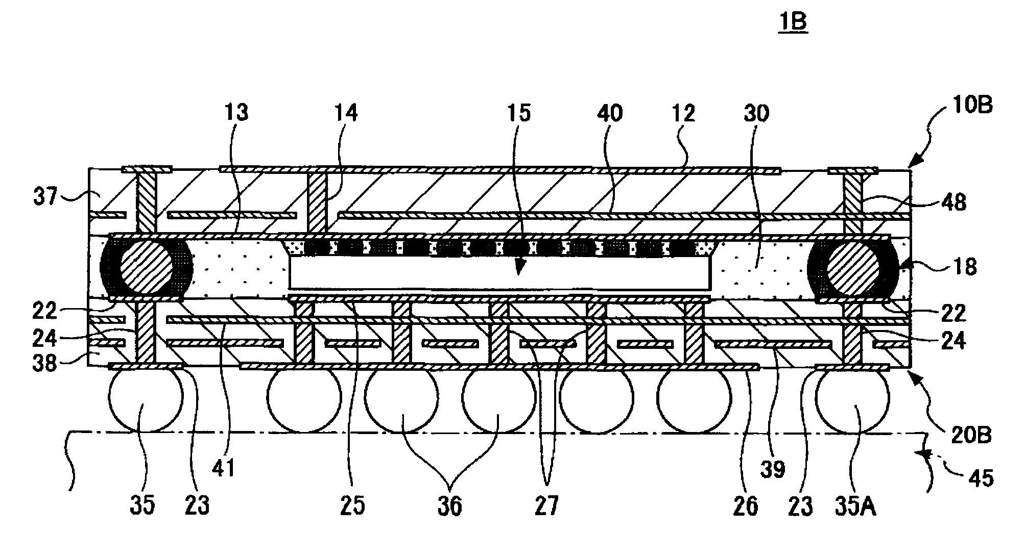
[0069]FIG. 4 shows an electronic apparatus 1B which is a second embodiment. In addition, components in FIG. 4 corresponding to the components shown in FIG. 3 are designated by the same reference numerals, and the description thereof is omitted.

[0070]In the electronic apparatus 1A related to the aforementioned first embodiment, double-sided printed circuit boards have been used as the first and second substrates 10A and 20A. In contrast, in this embodiment, multilayer wiring substrates are used as the first substrate 10B and the second substrate 20B.

[0071]The first substrate 10B is constructed such that three conductive layers are formed in an insulating layer 37. A conductive layer provided in the uppermost layer is used as the antenna 12. Further, a conductive layer formed in the lowermost layer is used as the wiring pattern 13. Also, a wiring layer formed in the middle layer is used as a ground layer 40.

[0072]The second substrate 20B is ...


PUM


Abstract

An electronic apparatus includes a semiconductor chip 15, a first substrate 10A having an antenna 12 formed on a first face 10a thereof and having the semiconductor chip 15 loaded on a second face 10b thereof, a second substrate 20A on which the first substrate 10A is provided so as to face the semiconductor chip 15, and which is connected to the outside, copper core solder balls 18 electrically connecting the first substrate 10A and the second substrate 20A, and a resin material 30 disposed between the first substrate 10A and the second substrate 20A. The second substrate 20A is provided with a thermal via 27 which radiates the heat in the semiconductor chip 15.

Description

BACKGROUND OF THE INVENTION[0001]The present invention relates to an electronic apparatus, and particularly, to an electronic apparatus having an antenna, and an electronic element which generates heat.[0002]With miniaturization of wireless communication apparatuses in recent years, miniaturization of electronic apparatuses to be loaded onto the wireless communication apparatuses is desired. As a miniaturized electronic apparatus, for example, one disclosed in Patent Document 1 is known. FIG. 1 is a view showing the schematic construction of the electronic apparatus 100 disclosed in Patent Document 1.[0003]The electronic apparatus 100 shown in this drawing is constituted by a substrate 110, a semiconductor chip 115, copper core solder balls 118, etc. The substrate 110 is a double-sided printed circuit board. An antenna 112 is formed on the top face of a substrate body 111, and a wiring pattern 113 is formed on the bottom face of the substrate body. The antenna 112 and the wiring pat...

Claims


Application Information

Patent Timeline
Patent Type & Authority Patents(United States)
IPC IPC(8): H05K7/20
CPCH01L23/3128H01L23/3677H01L23/49833H04B1/036H01Q1/2283H01L2924/15311H01L2924/15321H01L2924/19041H01L2924/3025H05K1/0206H05K1/185H01L2924/01087H01L2224/73204H01L2224/16225H01L2224/32225H01L2924/00H01L2224/73253H01L2223/6677H01L23/42H05K3/46
Inventor FUJII, TOMOHARU
Owner SHINKO ELECTRIC IND CO LTD
Why Eureka
Try Eureka