Semiconductor device comprising photoelectric conversion element and high-potential and low-potential electrodes

a technology of photoelectric conversion element and semiconductor device, which is applied in the direction of optical radiation measurement, pulse technique, instruments, etc., can solve the problems of reducing the detection range of light intensity, requiring a high power supply voltage, and generating parasitic resistance, so as to reduce the photosensitivity and reduce the generation of parasitic resistance , the effect of stable circuit operation

Inactive Publication Date: 2010-09-07
SEMICON ENERGY LAB CO LTD
View PDF57 Cites 16 Cited by
  • Summary
  • Abstract
  • Description
  • Claims
  • Application Information

AI Technical Summary

Benefits of technology

[0015]In view of the foregoing problems, it is an object of the invention to suppress a decrease in sensitivity of a photoelectric conversion device by suppressing parasitic resistance generated in a reference TFT of a current mirror circuit and preventing drops in gate voltage of the reference TFT.
[0022]According to the invention, a photoelectric conversion device in which a decrease in photosensitivity is suppressed can be provided. Further, since generation of parasitic resistance can be suppressed, stable circuit operation is ensured and products with high reliability can be provided.

Problems solved by technology

Many of conventional amplifier circuits have multi-stage configurations including a correction circuit, and thus require a high power supply voltage.
However, the above-described amplifier circuit having TFTs, e.g., a current mirror circuit, has a problem in that parasitic resistance is generated by a conductive layer which forms a TFT, wiring resistance of a wire connected thereto, contact resistance, or the like.
Regarding the current mirror circuit, in particular, there is a possibility that generation of parasitic resistance in a reference TFT will result in a decrease in detection range of light intensity.

Method used


Image

  • Semiconductor device comprising photoelectric conversion element and high-potential and low-potential electrodes
  • Semiconductor device comprising photoelectric conversion element and high-potential and low-potential electrodes
  • Semiconductor device comprising photoelectric conversion element and high-potential and low-potential electrodes

Examples


embodiment mode 1

[0057]Embodiment Mode 1 will be described below with reference to FIGS. 1 through 14C.

[0058]Note that the invention can be implemented in various different ways and it will be easily understood by those skilled in the art that various changes and modifications can be made in the invention without departing from the spirit and scope thereof. Therefore, the invention should not be construed as being limited to the description of the following embodiment modes.

[0059]Note also that in all the drawings illustrating embodiment modes, portions that are the same or portions having a similar function are denoted by the same reference numerals, and repetitive description thereof will be omitted.

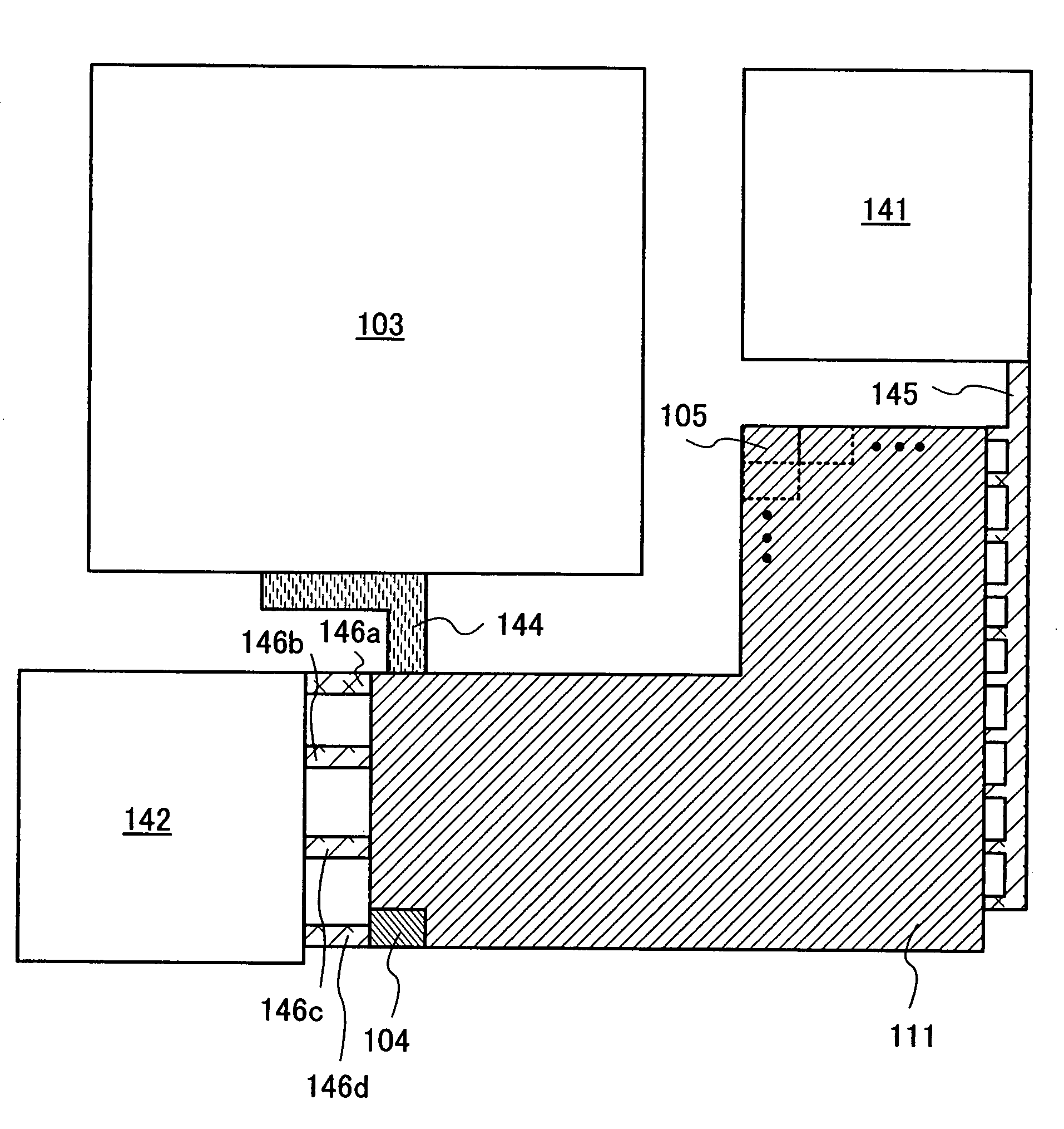
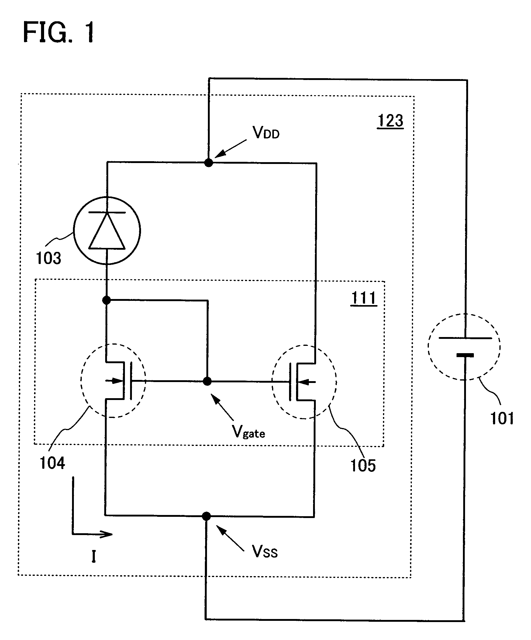
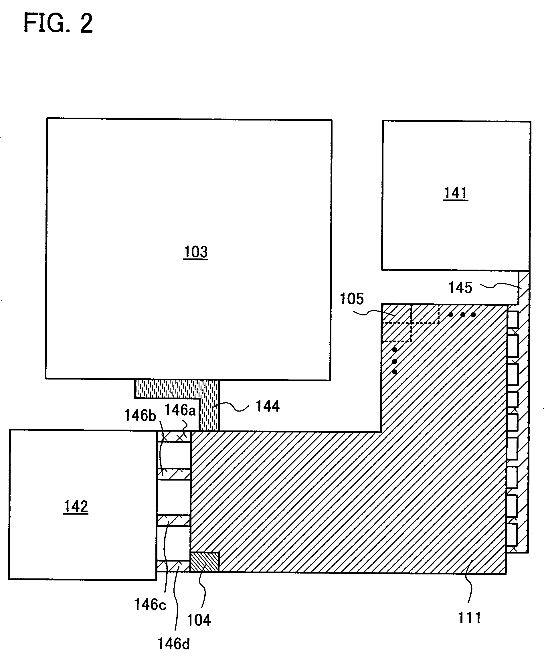
[0060]A semiconductor device of this embodiment mode includes, as shown in FIG. 1, a current mirror circuit 111 having transistors 104 and 105 and a power supply (bias) 101. In this embodiment mode, thin film transistors (TFTs) are used as the transistors 104 and 105. In addition, the TFTs 104 and 105 ...

embodiment mode 2

[0160]This embodiment mode will describe an example of an amplifier circuit constructed from p-channel TFTs with reference to FIGS. 9 and 15. Note that portions common to this embodiment and Embodiment Mode 1 are denoted by common reference numerals. Therefore, such portions may be formed through the same fabrication steps as those described in Embodiment Mode 1.

[0161]When an amplifier circuit, e.g., the current mirror circuit 203 is constructed from the p-channel TFTs 201 and 202, the impurity which imparts one conductivity type to the island-shaped semiconductor regions in Embodiment Mode 1 may be replaced with a p-type impurity, e.g., boron (B).

[0162]FIG. 9 is an equivalent circuit diagram of a photosensor in this embodiment mode in the case where the current mirror circuit 203 is constructed from the p-channel TFTs 201 and 202, and FIG. 15 is a cross-sectional view thereof.

[0163]In FIGS. 9 and 15, the terminal electrode 221 is electrically connected to the n-type semiconductor l...

embodiment mode 3

[0170]This embodiment mode will describe a photosensor and an amplifier circuit constructed from bottom-gate TFTs, and a method of fabricating them, with reference to FIG. 16A through 18. Note that portions common to this embodiment and Embodiment Modes 1 and 2 are denoted by common reference numerals.

[0171]First, a base insulating film 212 and a metal film 311 are formed over a substrate 210 (see FIG. 16A). In this embodiment mode, a stacked film of, for example, tantalum nitride with a thickness of 30 nm and tungsten (W) with a thickness of 370 nm is used as the metal film 311.

[0172]Besides, the metal film 311 can also be formed using a single-layer film made of an element selected from titanium (Ti), tungsten (W), tantalum (Ta), molybdenum (Mo), neodymium (Nd), cobalt (Co), zirconium (Zr), zinc (Zn), ruthenium (Ru), rhodium (Rh), palladium (Pd), osmium (Os), iridium (Ir), platinum (Pt), aluminum (Al), gold (Au), silver (Ag), or copper (Cu); a single-layer film made of an alloy ma...


PUM


Abstract

To suppress a decrease in photosensitivity of a photoelectric conversion element provided in a semiconductor device by reducing the parasitic resistance of an amplifier circuit. In addition, the amplifier circuit which amplifies the output current of the photoelectric conversion element is operated stably. A semiconductor device includes a photoelectric conversion element, a current mirror circuit having at least two thin film transistors, a high-potential power supply electrically connected to each of the thin film transistors, and a low-potential power supply electrically connected to each of the thin film transistors. When a reference thin film transistor is an n-type, the reference thin film transistor is placed closer to the low-potential power supply than an output thin film transistor is. When a reference thin film transistor is a p-type, the reference thin film transistor is placed closer to the high-potential power supply than an output thin film transistor is.

Description

BACKGROUND OF THE INVENTION[0001]1. Field of the Invention[0002]The present invention relates to photoelectric conversion devices and semiconductor devices having the same. In particular, the invention relates to a photoelectric conversion device having thin film semiconductor elements and a method of fabricating the same. Further, the invention also relates to an electronic device having such a photoelectric conversion device.[0003]2. Description of the Related Art[0004]There are known numerous photoelectric conversion devices that are used generally for detection of electromagnetic waves. For example, photoelectric conversion devices that detect ultraviolet rays to infrared rays are collectively referred to as photosensors. Among them, photosensors that detect visible light in the wavelength range of 400 to 700 nm are particularly referred to as visible light sensors. Many of such visible light sensors are used for devices whose illuminance and on / off switching need to be controll...

Claims


Application Information

Patent Timeline
Patent Type & Authority Patents(United States)
IPC IPC(8): H01L31/00
CPCG01J1/44H01L27/14632H01L27/1464H04N5/23241H04N5/2351H01L27/14687G01J2003/2836H04N23/65H04N23/71H01L31/09H03F3/08
Inventor HIROSE, ATSUSHI
Owner SEMICON ENERGY LAB CO LTD
Why Eureka
Try Eureka