Light emitting device, electronic appliance, and method for manufacturing light emitting device

a technology of light emitting devices and electronic appliances, which is applied in the manufacture of electrode systems, discharge tubes luminescnet screens, electric discharge tubes/lamps, etc., can solve the problems of lowering luminance of light emitting elements, and easy deterioration of el materials for forming el layers, so as to prevent moisture from entering the light emitting elements

Active Publication Date: 2010-09-07
SEMICON ENERGY LAB CO LTD
View PDF32 Cites 50 Cited by
  • Summary
  • Abstract
  • Description
  • Claims
  • Application Information

AI Technical Summary

Benefits of technology

[0011]It is an object of the present invention to provide a light emitting device with a structure in which a light emitting element is sandwiched by two substrates to prevent moisture from penetrating into the light emitting element, and a method for manufacturing the same. It is another object of the invention to control a gap between the two substrates precisely.

Problems solved by technology

An EL material for forming an EL layer is very easily deteriorated.
In particular, the EL material is easily deteriorated due to existence of oxygen or moisture, and therefore, the EL material had drawbacks in which luminance of a light emitting element is lowered and life thereof is shortened.

Method used


Image

  • Light emitting device, electronic appliance, and method for manufacturing light emitting device
  • Light emitting device, electronic appliance, and method for manufacturing light emitting device
  • Light emitting device, electronic appliance, and method for manufacturing light emitting device

Examples


embodiment mode 1

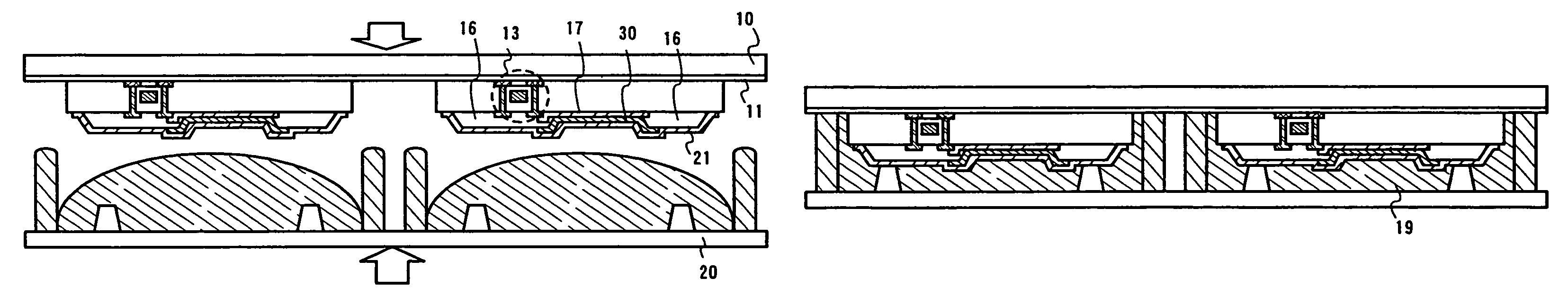
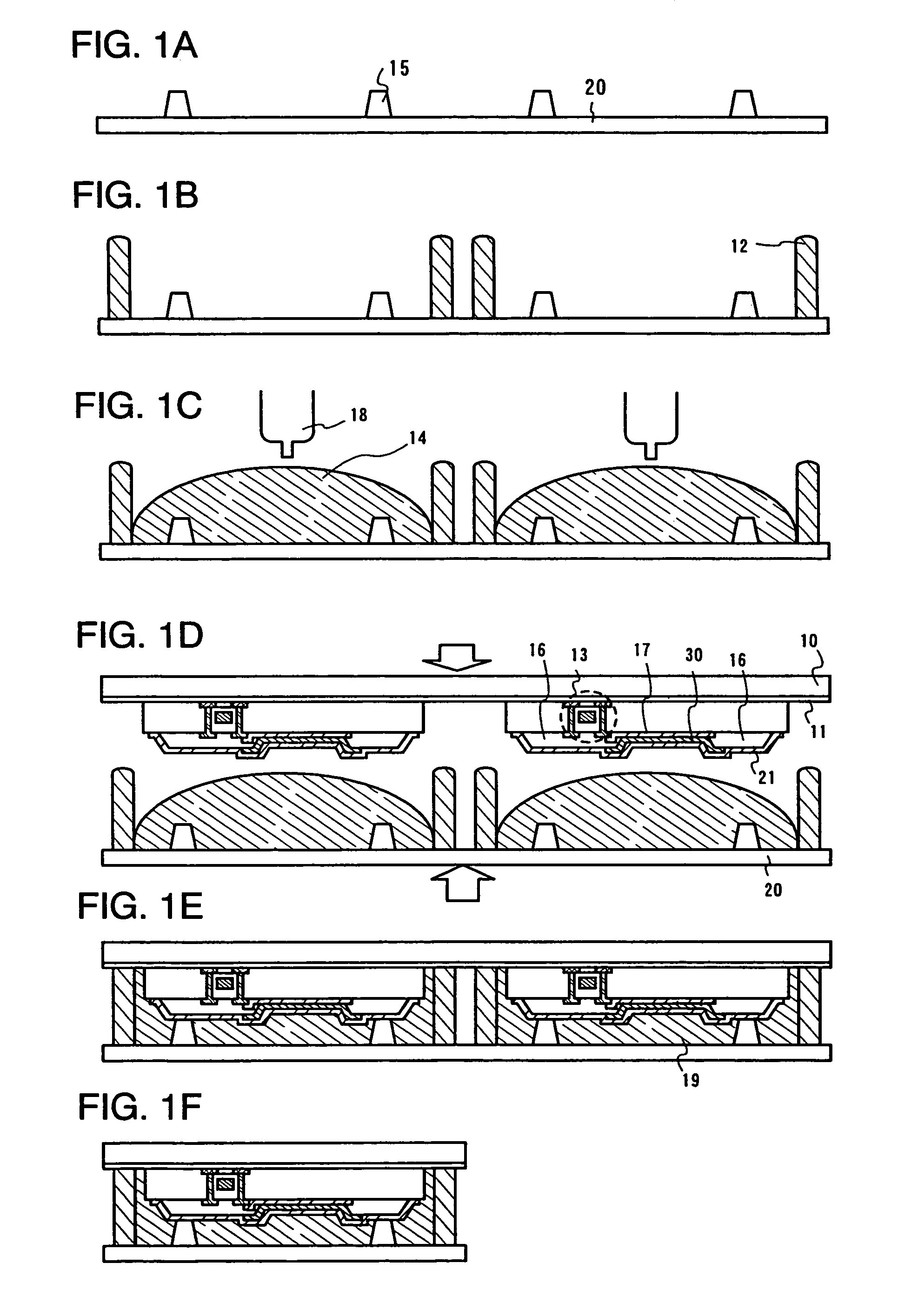
[0059]The present embodiment mode will explains a method for manufacturing a light emitting device in the case of the multiple pattern in which a pair of attached substrates is divided into multiple patterns (e.g., two pieces of panels are manufactured from a pair of attached substrates) with reference to FIGS. 1A to 1F.

[0060]A second substrate 20 that will serve as a sealing substrate is prepared. Columnar spaces 15 are formed on the second substrate 20 (FIG. 1A). The columnar spacers 15 are formed by patterning a level film in predetermined portions. The height of the columnar spacers 15 is important, and determines a gap between two substrates. Although the columnar spacers are exemplified as structures for maintaining the gap therebetween, the spacers may have a wall-shaped structure or a grid-like structure, or a combination of such shapes.

[0061]The columnar spacers may contain a drying agent.

[0062]Patterns of a sealing material 12 is formed by using a dispenser device, a dropl...

embodiment mode 2

[0078]A method for manufacturing a dual-emission type display device will be described with reference to FIG. 5.

[0079]A base insulating film is formed on a substrate 400. In order to extract light from the substrate 400 as a display screen, a substrate with a light transmitting property such as a glass substrate and a quartz substrate may be used as the substrate 400. A heat-resistant plastic substrate with a light transmitting property that can withstand a processing temperature can also be employed. A glass substrate is, herein, used as the substrate 400. The refractive index of the glass substrate is approximately 1.55.

[0080]As the base insulating film, a base film made from a silicon oxide film, a silicon nitride film, a silicon oxynitride film, and the like is formed. The base insulating film has light transmitting properties. Although the base insulating film has, herein, two-layer structure, it may have a single layer or two or more layers of the above insulating films. Note ...

embodiment 1

[0132]In the present embodiment, FIG. 8 shows an example of a manufacturing device that is partly different of those in FIGS. 6 and 7.

[0133]As well as FIG. 6 and FIG. 7, the manufacturing device as shown in FIG. 8 includes: the transport chamber 108 for transporting a substrate to the delivery chamber 111; the delivery chamber 107; the gates 100j, and 100n to 100s; and the film formation chambers 109, 110, 113, and 132. In the embodiment, the portions identical to those in FIG. 6 and FIG. 7 will not be further explained for the sake of simplification. To prevent moisture from adhering, an inert gas (e.g., nitrogen gas) having a controlled dew point is preferably filled in the chambers (including the delivery chamber, the processing chamber, the transport chamber, a film formation chamber, etc.), other than an unloading chamber 219 and a sealing substrate loading chamber 217. Preferably, pressure in such chambers filled with an inert gas is kept under reduced pressure.

[0134]In FIG. 8...


PUM


Abstract

To provide a light emitting device that has a structure in which a light emitting element is sandwiched by two substrates to prevent moisture from penetrating into the light emitting element, and a method for manufacturing thereof. In addition, a gap between the two substrates can be controlled precisely. In the light emitting device according to the present invention, an airtight space surrounded by a sealing material with a closed pattern is kept under reduced pressure by attaching the pair of substrates under reduced pressure. A columnar or wall-shaped structure is formed between light emitting regions inside of the sealing material, in a region overlapping with the sealing material, or in a region outside of the sealing material so that the gap between the pair of substrates can be maintained precisely.

Description

BACKGROUND OF THE INVENTION[0001]1. Field of the Invention[0002]The present invention relates to an organic light emitting element comprising an anode, a cathode, and a layer containing an organic compound that emits light by being applied with an electric field (hereinafter, referred to as an electroluminescent layer), and a light emitting device using the same. In particular, the invention relates to an electronic appliance mounted with a light emitting display device, which comprises a TFT and an organic light emitting element, as a component part.[0003]In the present specification, a light emitting device indicates an image display device, a light emitting device, a light source (including a lighting device), and the like. The light emitting device further includes all of a module in which a light emitting device is attached with a connector, e.g., an FPC (flexible printed circuit), a TAB (tape automated bonding) tape, or a TCP (tape carrier package); a module having a printed w...

Claims


Application Information

Patent Timeline
Patent Type & Authority Patents(United States)
IPC IPC(8): H01J9/00H05B33/04H01L27/32H01L51/00H01L51/52H05B33/00
CPCH01L51/525H01L33/52H01L51/5237H01L27/3211H01L27/3244H01L51/0005H01L51/56H01L2227/323H01L2251/5323H01L2251/566H10K59/35H10K71/135H10K59/12H10K50/8428H10K50/846H10K50/8426H10K2102/3031H10K59/1201H10K71/851H10K71/00H10K50/11H10K50/81H10K50/82H10K50/84H10K50/865H10K50/868H10K59/123H10K71/50H10K2102/101H01L27/0248
Inventor HIRAKATA, YOSHIHARUYAMAZAKI, SHUNPEI
Owner SEMICON ENERGY LAB CO LTD
Why Eureka
Try Eureka