Unlock instant, AI-driven research and patent intelligence for your innovation.

Interface for transferring debug information

Inactive Publication Date: 2010-09-07
STMICROELECTRONICS LTD
View PDF70 Cites 23 Cited by
  • Summary
  • Abstract
  • Description
  • Claims
  • Application Information

AI Technical Summary

Benefits of technology

[0009]These and other drawbacks of conventional debug systems are overcome by providing a dedicated link which operatively couples a processor and a debug circuit which transfers information between them to support debugging operations. In one aspect, the processor provides information that a debug trace tool would need to be performed non-intrusively, that is, without disturbing memory accesses or the execution pipeline of the processor. Also, in one aspect, information is transmitted from the processor at a rate that matches the processor internal clock speed.
[0010]In one aspect, the processor communicates over this link to a debug circuit. Further, this link coupling the processor and the debug circuit is utilized in a manner which minimizes a number of physical lines required to communicate the information. Further, information needed to perform trace operations is transferred in a non-intrusive manner over the link. In one aspect, the processor and debug circuit may be located on a single integrated circuit.
[0012]According to one aspect of the invention, increment of program counter signals to the debug circuit to allow the circuit to track the program counter in the processor. Thus, transmission of the entire program counter is not necessary and the number of communication lines between the processor and debug circuit is minimized.
[0015]In another aspect of the invention, the processor provides process identification information to debug circuit which then can base / optimize filtering based on process identifier values in debug circuit. In one aspect, the process identification information is transferred over lines dedicated for trace data in order to minimize the number of communication lines.
[0016]Further, the debug circuit may provide a stall control signal to stall the processor. Advantageously, trace information is preserved in situations when the debug circuit cannot accept additional trace information. Further, the processor may provide an indication that the processor has stalled. Also, the debug circuit may provide exception indication signals to indicate that an exception occurred in debug unit.

Problems solved by technology

Because multiple modules and their communications occur internally to the chip, access to this information is generally difficult when problems occur in software or hardware.
Thus, debugging on these systems is not straightforward.
However, debugging an SOC generally involves intrusively monitoring one or more processor registers or memory locations.
Accesses to memory locations are sometimes destructive, and a data access to a location being read from a debugging tool may impede processor performance.
Similarly, accesses are generally performed over a system bus to the processor, memory, or other module, and may reduce available bandwidth over the system bus for performing general operations.
By slowing or pausing the processor, some types of errors may not be reproduced, and thus cannot be detected or corrected.
Further, accurate information may not be available altogether due to a high speed of the processor; information may be skewed or missing.
However, these units affect the operation of the processor when obtaining information such as trace information.
These devices typically function at a lower speed than the processor, and thus affect processor operations when they access processor data.
Thus, the presence of the debug code is intrusive in terms of memory layout, and instruction stream disruption.
However, emulators are prohibitively expensive for some applications, and do not successfully match all on-chip speeds or communications.
Thus, emulator systems are inadequate.
Further, these systems generally transfer information over the system bus, and therefore necessarily impact processor performance.
LSA devices are generally expensive devices, and do not allow access to pin information inside the chip.
In sum, there are many systems which are inadequate for monitoring the internal states of a processor and for providing features such as real-time state and real-time trace in a non-intrusive mariner.

Method used


Image

  • Interface for transferring debug information
  • Interface for transferring debug information
  • Interface for transferring debug information

Examples


Embodiment Construction

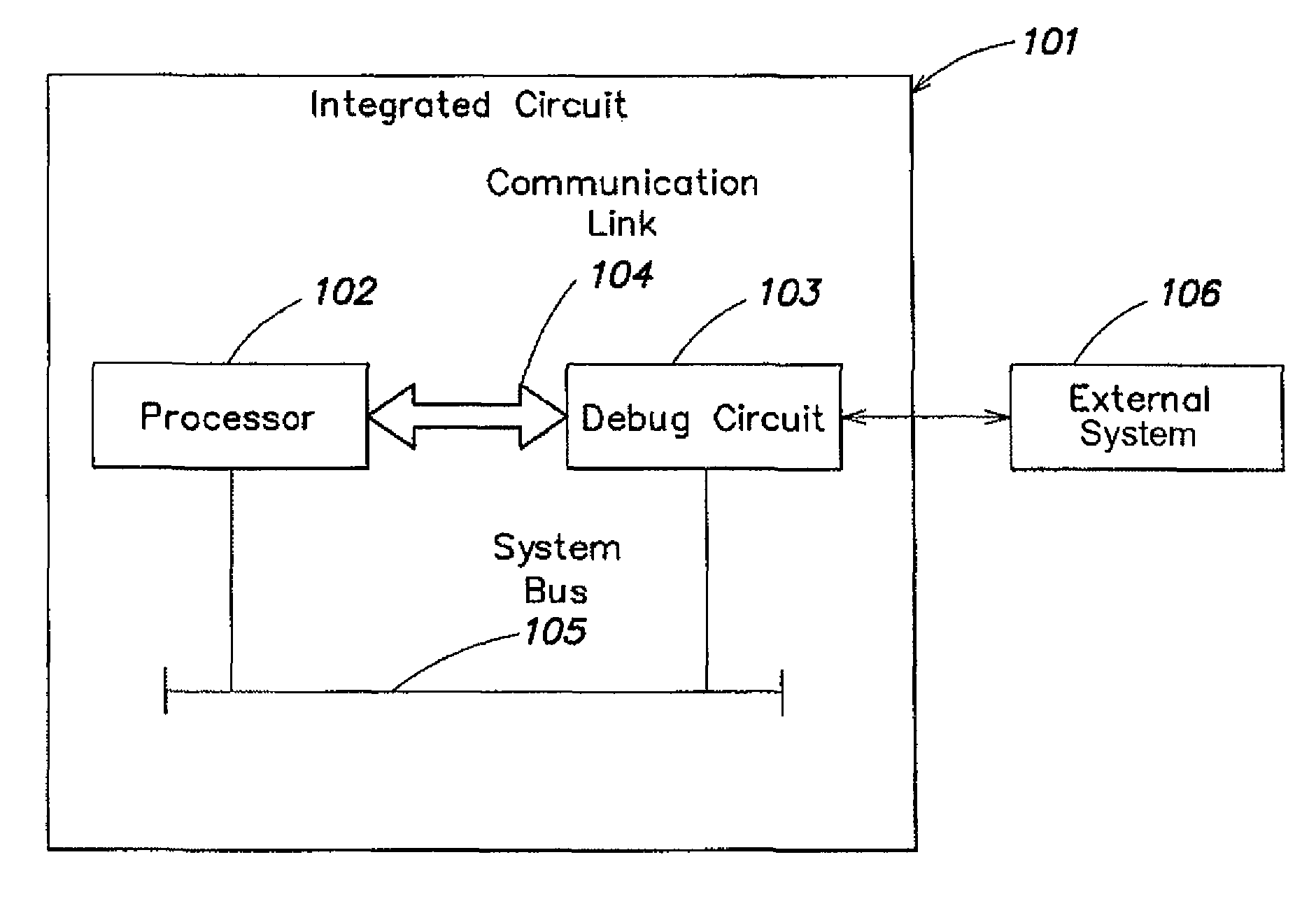
[0035]One embodiment of the invention is described with particularity with respect to FIG. 1. FIG. 1 shows a block diagram of an integrated circuit device 101, or system-on-chip (SOC) mentioned above. This circuit may include a processor 102 and debug circuit 103 or module interconnected by a system bus 105. System bus 105 may be, for example, a conventional processor bus, packet switch, or other communication medium used to communicate operating information between modules of device 101. Operations such as reads, writes, swaps, and the like are typical operations that are performed between modules.

[0036]Processor 102 is a device which is adapted to read and execute one or more processor instructions, and to perform operations on data. Processor 102 may read data from a number of data sources (not shown), and write data to one or more data stores (not shown). These data sources and stores may include Random Access Memory (RAM), a computer hard disc accessible through a hard disc con...


PUM


Abstract

An microcomputer is provided including a processor and a debug circuit including a dedicated link which transfers information between the processor and debug circuit to support debugging operations. In one aspect, the processor provides program counter information, which is stored in a memory-mapped register of the debug circuit. The program counter information may be a value of the processor program counter at a writeback stage of a processor pipeline. Also, trace information including message information is transferred in a non-intrusive manner over the dedicated link. In one aspect, the microcomputer is implemented as a single integrated circuit.

Description

BACKGROUND OF THE INVENTION[0001]1. Field of the Invention[0002]The invention relates generally to debugging processors, and more specifically, to an interface for transferring debug information.[0003]2. Related Art[0004]System-on-chip devices (SOCs) are well-known. These devices generally include a processor, one or more modules, bus interfaces, memory devices, and one or more system busses for communicating information. Because multiple modules and their communications occur internally to the chip, access to this information is generally difficult when problems occur in software or hardware. Thus, debugging on these systems is not straightforward. As a result of development of these SOCs, specialized debugging systems have been developed to monitor performance and trace information on the chip. Such systems typically include dedicated hardware or software such as a debug tool and debug software which accesses a processor through serial communications.[0005]However, debugging an SO...

Claims


Application Information

Patent Timeline
IPC IPC(8): G06F9/44G06F11/28G06F11/22G06F11/26G06F11/36G06F15/78
CPCG06F11/3636G06F11/3656G06F11/261
Inventor EDWARDS, DAVID ALANGEARTY, MARGARET ROSEFARRALL, GLENN A.HASEGAWA, ATSUSHIRICH, ANTHONY WILLIS
Owner STMICROELECTRONICS LTD
Features
  • R&D
  • Intellectual Property
  • Life Sciences
  • Materials
  • Tech Scout
  • Unparalleled Data Quality
  • Higher Quality Content
  • 60% Fewer Hallucinations
Learn More