Manufacturing methods of SOI substrate and semiconductor device

a manufacturing method and technology of silicon wafer, applied in semiconductor/solid-state device manufacturing, basic electric elements, electric devices, etc., can solve the problems of limited availability and the size of silicon wafers dependent on manufacturing, and achieve low power consumption, high speed driving, and large display portions

Inactive Publication Date: 2010-09-14
SEMICON ENERGY LAB CO LTD
View PDF25 Cites 12 Cited by
  • Summary
  • Abstract
  • Description
  • Claims
  • Application Information

AI Technical Summary

Benefits of technology

[0013]In the present invention, by the ion implantation separation method, a second seed substrate having a first separation layer in which ions are implanted at a predetermined depth is bonded to a first seed substrate, and then is separated therefrom with the first separation layer used as a cleavage plane, whereby a single crystalline semiconductor film having a discontinuous portion can be formed. Further, a new single crystalline semiconductor film is formed by an epitaxial growth method using the single crystalline semiconductor film having a discontinuous portion and the first seed substrate as a seed, and thus a large-area continuous single crystalline semiconductor film can be formed. Then, by an ion implantation separation method, ions are implanted again at a predetermined depth of the large-area single crystalline semiconductor film to form a second separation layer and the large-area single crystalline semiconductor film is bonded to a large-area glass substrate. Then, the single crystalline semiconductor film is separated from the glass substrate with the second separation layer used as a cleavage plane, and thus a large-area single crystalline semiconductor film can be formed over the glass substrate.
[0021]According to the present invention, when a single crystalline semiconductor film is formed by SOI technique, a large-area single crystalline semiconductor film can be formed without any space between single crystalline semiconductor films. Thus, even if a substrate having an insulating surface is larger, a large-area continuous single crystalline semiconductor film in accordance with the expansion of the substrate size can be formed. Accordingly, an SOI substrate having a large-area single crystalline semiconductor film can be formed. In addition, by using an SOI substrate of the present invention, it is possible that a semiconductor device and the like with high speed driving, low power consumption and a large display portion is formed.

Problems solved by technology

However, the size of a silicon wafer is dependent on a manufacturing method thereof, and is limited unfortunately.
As a result, there is a problem in that a gap between a single crystalline semiconductor film and another single crystalline semiconductor film adjacent thereto, which have been bonded to the glass substrate, and in the gap, no single crystalline semiconductor film exist.

Method used


Image

  • Manufacturing methods of SOI substrate and semiconductor device
  • Manufacturing methods of SOI substrate and semiconductor device
  • Manufacturing methods of SOI substrate and semiconductor device

Examples


embodiment mode 1

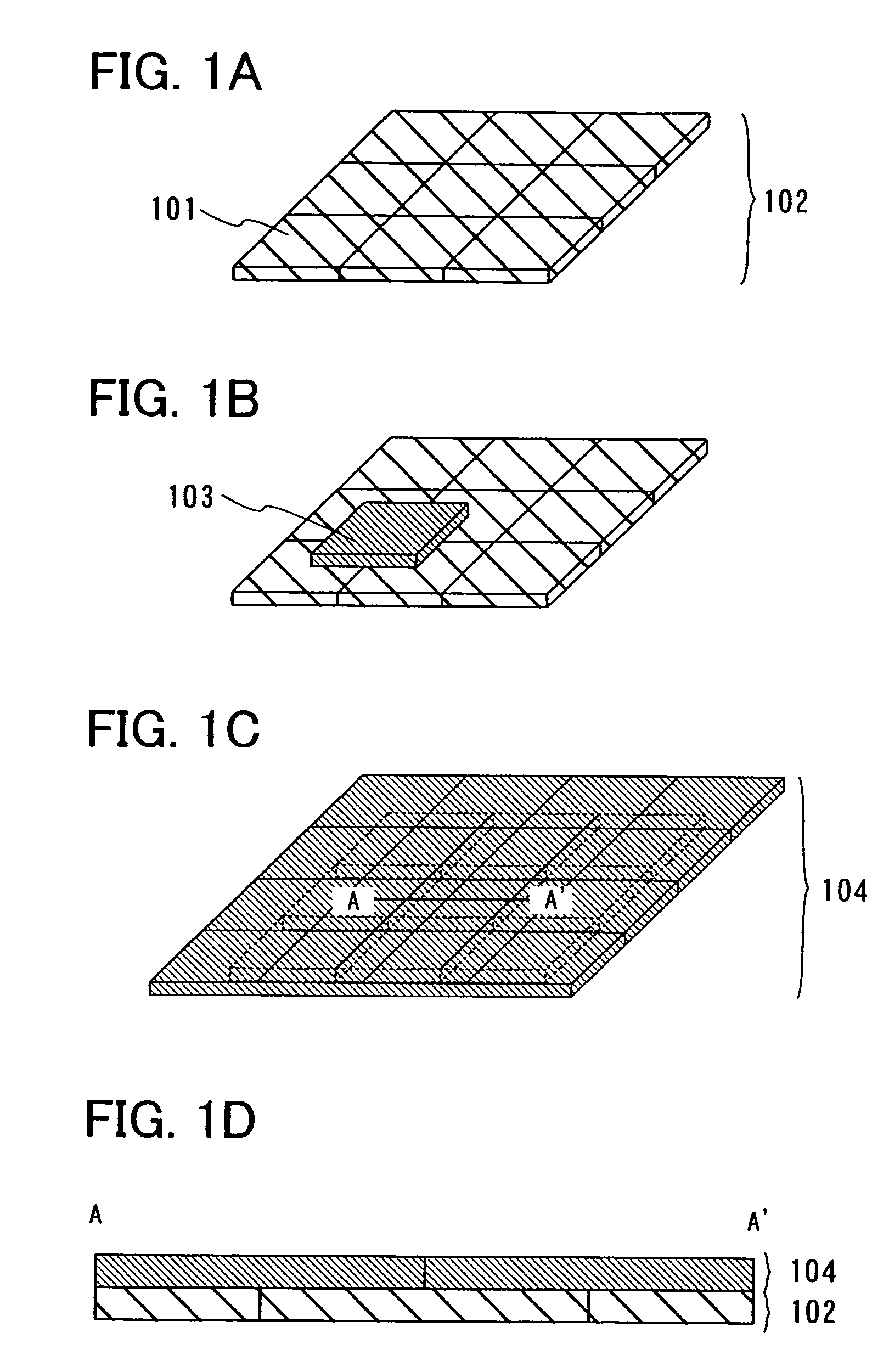
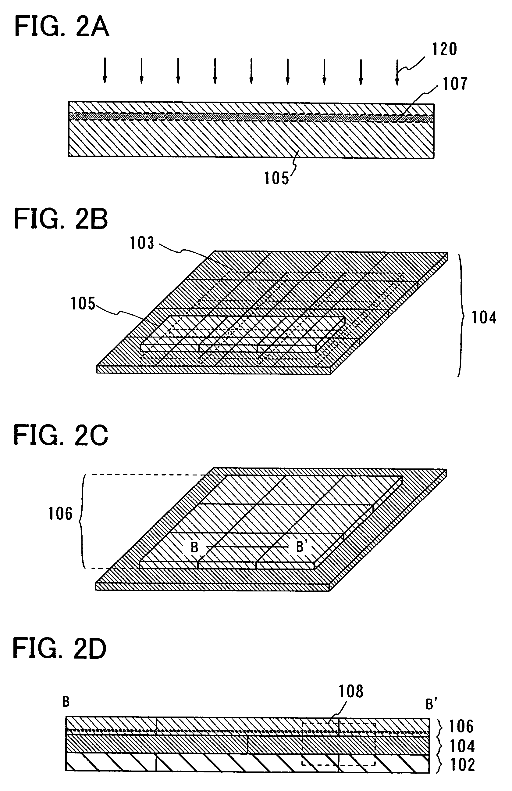
[0039]In Embodiment Mode 1, a manufacturing method of an SOI substrate according to the present invention is described with reference to FIGS. 1A to 1D, FIGS. 2A to 2D, FIGS. 3A to 3D and FIGS. 4A to 4D.

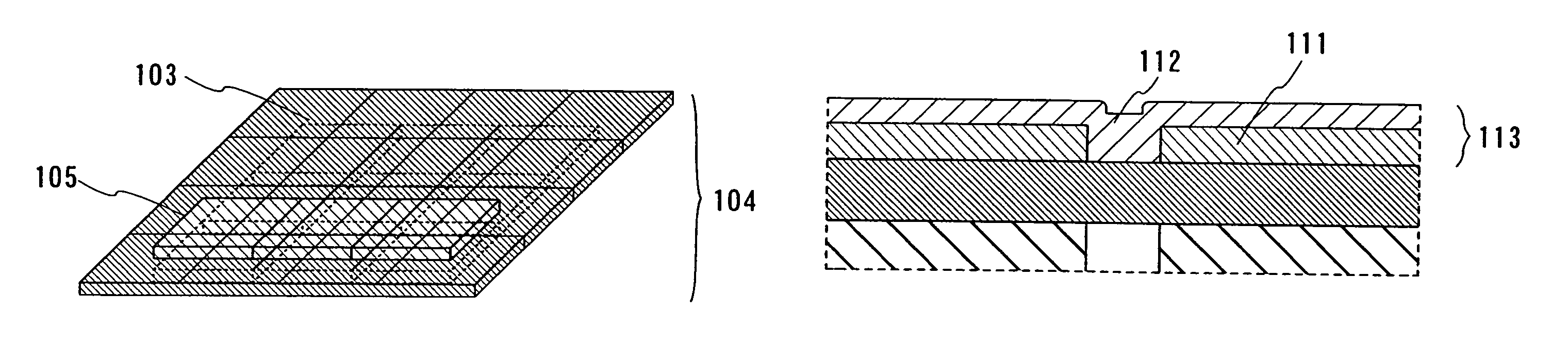
[0040]As illustrated in FIG. 1A, a plurality of silicon wafers 101 with the same thickness, obtained by slicing an ingot of a single crystalline semiconductor are tightly arranged without any space therebetween on a plane surface. In Embodiment Mode 1, nine silicon wafers 101 having a side of 5 inches are arranged to form a fixing substrate 102. Note that the number of the silicon wafers constituting the fixing substrate 102 is not limited to nine, and may be increased or decreased as appropriate. In addition, the shape of the silicon wafers constituting the fixing substrate 102 is not limited to a square shape, and may be circular or rectangular. Further, as a material of the fixing substrate 102, a silicon wafer is not a limiting example, and any material which can fix a first seed...

embodiment mode 2

[0067]In Embodiment Mode 2, a manufacturing method of an SOI substrate according to the present invention is described with reference to FIGS. 5A to 5D and FIGS. 6A to 6D.

[0068]Similarly to Embodiment Mode 1, a plurality of silicon wafers 201 with the same thickness are prepared, which are obtained by slicing an ingot of a single crystalline semiconductor. A bonding film 202 is formed over each of the silicon wafers 201. Note that for the bonding film 202, a silicon oxide film having excellent planarity is suitable. In particular, a silicon oxide film formed by a chemical vapor deposition method using an organic silane gas is preferable. Examples of an organic silane gas include gases of silicon-containing compounds such as tetraethoxysilane, tetramethylsilane, tetramethylcyclotetrasiloxane, octamethylcyclotetrasiloxane, hexamethyldisilazane, triethoxysilane, or trisdimethylaminosilane.

[0069]Next, the plurality of silicon wafers 201 provided with the bonding film 202 are tightly arr...

embodiment mode 3

[0089]In Embodiment Mode 3, a manufacturing method of a semiconductor device according to the present invention, using an SOI substrate described in Embodiment Mode 1 or 2, is described with reference to FIGS. 7A to 7D, FIGS. 8A to 8D, and FIG. 9.

[0090]First, a single crystalline semiconductor film formed over a substrate 701 by the method described in Embodiment Mode 1 or Embodiment Mode 2 is etched, so that element separation is conducted in accordance with arrangement of semiconductor elements, and semiconductor films 702 are formed. Note that the substrate 701 is a substrate having an insulating surface or an insulating substrate, and all types of substrates for the electronics industry, e.g., glass substrates such as aluminosilicate glass, aluminoborosilicate glass, and bariumborosilicate glass; quartz glass; plastic substrates, and the like can be used.

[0091]In addition, although not illustrated here, an insulating film serving as a base film may be formed over the substrate 7...


PUM


Abstract

A manufacturing method of an SOI substrate and a manufacturing method of a semiconductor device are provided. When a large-area single crystalline semiconductor film is formed over an enlarged substrate having an insulating surface, e.g., a glass substrate by an SOI technique, the large-area single crystalline semiconductor film is formed without any gap between plural single crystalline semiconductor films, even when plural silicon wafers are used. An aspect of the manufacturing method includes the steps of disposing a first seed substrate over a fixing substrate; tightly arranging a plurality of single crystalline semiconductor substrates over the first seed substrate to form a second seed substrate; forming a large-area continuous single crystalline semiconductor film by an ion implantation separation method and an epitaxial growth method; forming a large-area single crystalline semiconductor film without any gap over a large glass substrate by an ion implantation separation method again.

Description

BACKGROUND OF THE INVENTION[0001]1. Field of the Invention[0002]The present invention relates to a manufacturing method of a silicon-on-insulator (SOI) substrate and a manufacturing method of a semiconductor device using the SOI substrate. In particular, the present invention relates to a technique by which a large area single crystalline semiconductor film is formed over a substrate having an insulating surface such as glass by an SOI bonding technique.[0003]2. Description of the Related Art[0004]In recent years, a technique for forming a semiconductor device such as a thin film transistor (TFT) using a semiconductor thin film (the thickness of several nanometers to several hundreds nanometers) formed over a substrate having an insulating surface such as glass has been attracted. Thin film transistors are widely applied to electronic devices such as an IC and an electro-optical device. In particular, urgent development is required on thin film transistors as switching elements of i...

Claims


Application Information

Patent Timeline
Patent Type & Authority Patents(United States)
IPC IPC(8): H01L21/30
CPCH01L21/76254H01L21/20
Inventor MORIWAKA, TOMOAKI
Owner SEMICON ENERGY LAB CO LTD
Why Eureka
Try Eureka