Top-emission active matrix electroluminescence device and method for fabricating the same

a technology of active matrix and electroluminescence device, which is applied in the direction of discharge tube luminescence screen, identification means, instruments, etc., can solve the problems of reducing durability, reducing reliability of device, short circuit or oxidation of metal common electrodes, etc., and enhancing luminous efficiency and improving electrical function of devi

Active Publication Date: 2010-09-28
LG DISPLAY CO LTD
View PDF24 Cites 5 Cited by
  • Summary
  • Abstract
  • Description
  • Claims
  • Application Information

AI Technical Summary

Benefits of technology

[0010]An object of the present invention is to provide a top-emission active matrix electroluminescence device and a method for fabricating the same that can simultaneously enhance the luminous efficiency and improve the electrical function of the device.

Problems solved by technology

However, if the metal common electrode is formed too thin, the heat applied thereon may cause the metal common electrode to be short-circuited or oxidized.
Thus, the reliability of the device is lowered and the durability is reduced.

Method used


Image

  • Top-emission active matrix electroluminescence device and method for fabricating the same
  • Top-emission active matrix electroluminescence device and method for fabricating the same
  • Top-emission active matrix electroluminescence device and method for fabricating the same

Examples


first embodiment

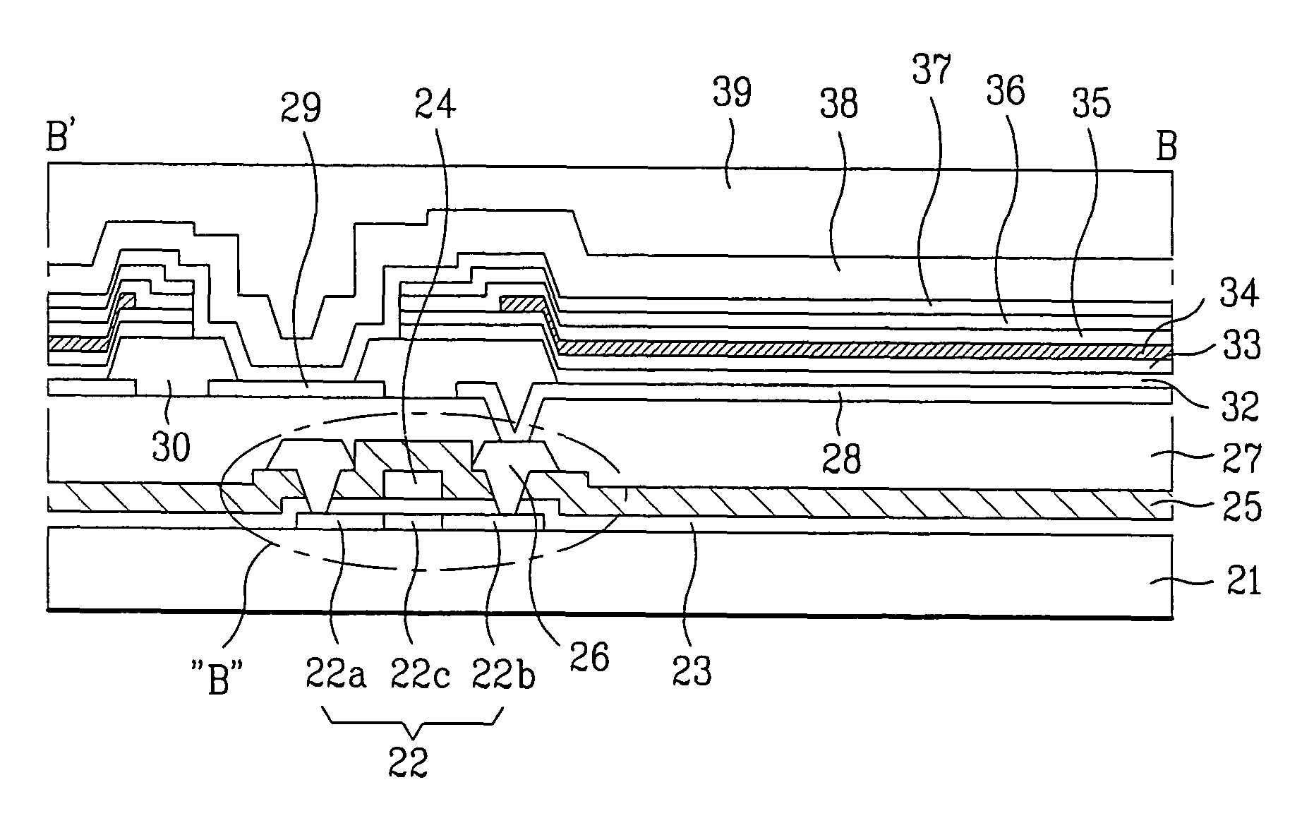
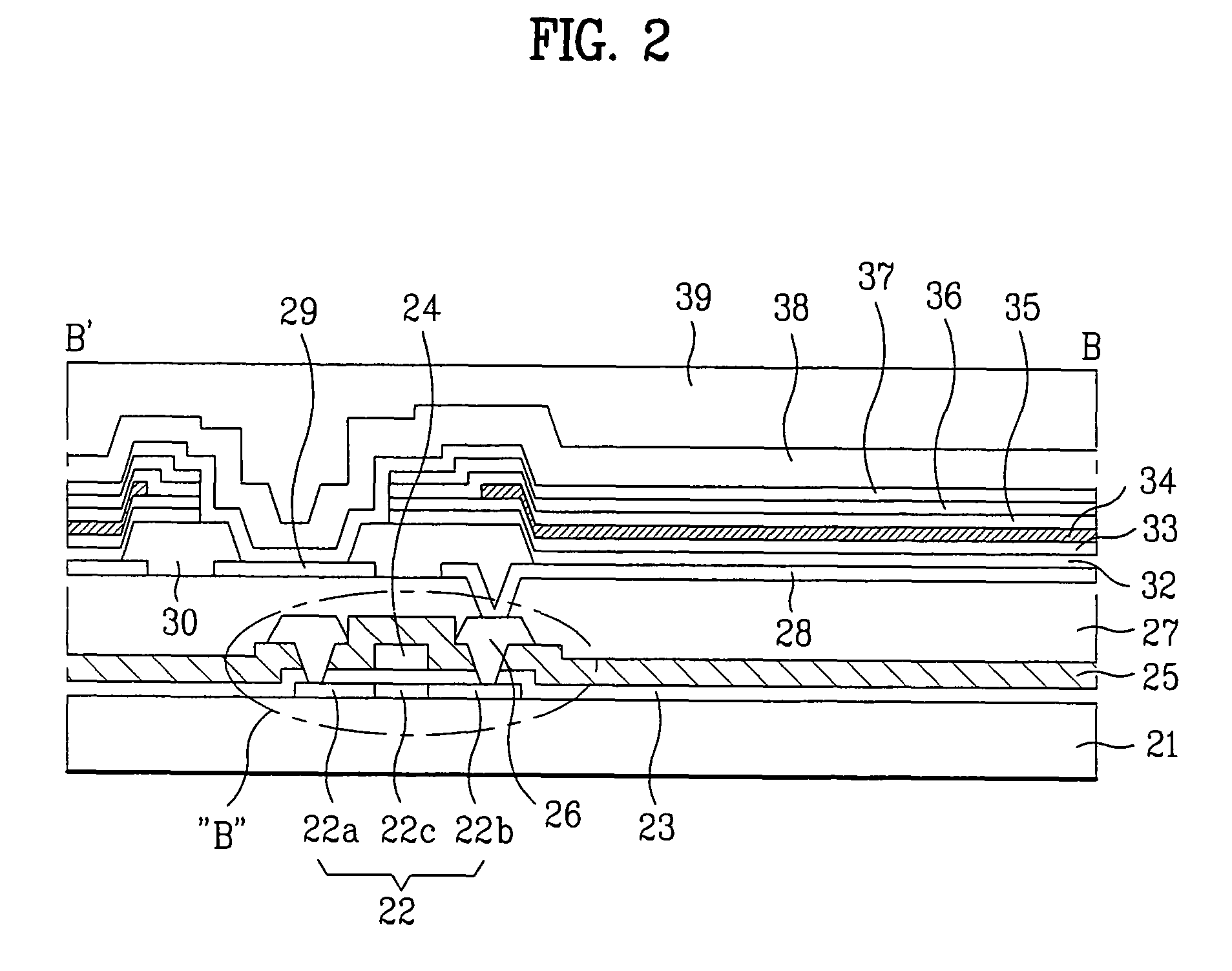
[0041]FIGS. 3A to 3G illustrate the process steps of a method for fabricating the active matrix electroluminescence device according to a first embodiment of the present invention. Referring to FIG. 3A, in order to be used as an active layer of the thin film transistor B, the semiconductor layer 22 is formed on the glass substrate 21 by using a polycrystalline silicon. Subsequently, the semiconductor layer 22 is patterned to leave only a portion of the semiconductor layer 22, corresponding to the area on which the thin film transistor B is to be formed. Then, the gate insulating layer 23 is deposited on the entire surface of the glass substrate 21 and the semiconductor layer 22, and a conductive material layer is deposited on the gate insulating layer 23, so as to form the gate electrode. The conductive material layer is patterned so that only a predetermined portion remains on the patterned semiconductor layer 22, thereby forming the gate electrode 24.

[0042]Thereafter, the gate ele...

second embodiment

[0054]FIGS. 5A to 5F illustrate the process steps of a method for fabricating the active matrix electroluminescence device according to a second embodiment of the present invention. Referring to FIG. 5A, the semiconductor layer 122 is formed on the glass substrate 121 in order to be used as an active layer of the thin film transistor B. The semiconductor layer 122 is made of poly-silicon. Subsequently, the semiconductor layer 122 is patterned to leave only a portion of the semiconductor layer 122, corresponding to the area on which the thin film transistor B is to be formed. Then, the gate insulating layer 123 is deposited on the entire surface of the glass substrate 121 and the semiconductor layer 122, and a conductive material layer is deposited on the gate insulating layer 123, so as to form the gate electrode. The conductive material layer is patterned so that only a predetermined portion remains on the patterned semiconductor layer 122, thereby forming the gate electrode 24.

[00...


PUM

PropertyMeasurementUnit
thicknessaaaaaaaaaa
thicknessaaaaaaaaaa
thicknessaaaaaaaaaa

Abstract

A top-emission active matrix electroluminescence device and a method for fabricating the same are disclosed, wherein a counter common electrode is formed in an area outside of a pixel area, when forming a pixel electrode, so as to simultaneously enhance an emission efficiency and an electrical function of the device. Herein, the counter common electrode is electrically connected to a common electrode, thereby preventing an overload and a short-circuit of the common electrode, even though the common electrode is formed in a thin layer.

Description

CROSS-REFERENCE TO RELATED APPLICATIONS[0001]This application claims the benefit of Korean Application Nos. P2003-054149, filed on Aug. 5, 2003, and P2003-054150, filed on Aug. 5, 2003, which is hereby incorporated by reference as if fully set forth herein.BACKGROUND OF THE INVENTION[0002]1. Field of the Invention[0003]The present invention relates to an organic electroluminescence device, and more particularly, to a top-emission active matrix electroluminescence device and a method for fabricating the same. Although the present invention is suitable for a wide scope of applications, it is particularly suitable for enhancing the luminous efficiency and improving the electrical function of the device.[0004]2. Discussion of the Related Art[0005]An electroluminescence device is being viewed as a next generation flat display device for its characteristics of a wide viewing angle, a high aperture ratio, and a high chromaticity. More specifically, in an organic electroluminescence (EL) de...

Claims


Application Information

Patent Timeline
Patent Type & Authority Patents(United States)
IPC IPC(8): H05B33/00H05B33/26G09F9/30H01L27/15H01L27/32H01L51/50H01L51/52H05B33/10H05B33/12H05B33/14H05B33/20H05B33/24
CPCH01L27/3244H01L51/5228H01L51/5234H01L27/3211H01L2251/5315H10K59/35H10K59/1315H10K50/824H10K50/828H10K59/1201H10K2102/3026H10K59/12
Inventor KIM, HONG GYU
Owner LG DISPLAY CO LTD
Why Eureka
Try Eureka