Unlock instant, AI-driven research and patent intelligence for your innovation.

Flash memory device capable of overcoming fast program/slow erase phenomenon and erase method thereof

a flash memory and program technology, applied in static storage, digital storage, instruments, etc., can solve the problems of further weakening reducing the area of the tunnel oxide layer, and difficult to use a high erase voltage, so as to improve the e/w cycling characteristic

Inactive Publication Date: 2010-10-05
SK HYNIX INC
View PDF15 Cites 16 Cited by
  • Summary
  • Abstract
  • Description
  • Claims
  • Application Information

AI Technical Summary

Benefits of technology

[0013]Accordingly, the present invention relates to a flash memory device and an erase method thereof, in which an erase characteristic (E / W cycling characteristic) can be improved.

Problems solved by technology

However, as the size of a cell shrinks, the area of the tunnel oxide layer is decreased, thereby further weakening the E / W cycling characteristic.
It makes it difficult to use a high erase voltage.
First, since the erase operation is repeated several times while increasing the voltage difference between the control gate and the well region, an overall erase operating time increases.
Next, if the voltage difference between the control gate and the well region is increased so as to reduce the erase operating time, the E / W cycling characteristic will deteriorate.

Method used


Image

  • Flash memory device capable of overcoming fast program/slow erase phenomenon and erase method thereof
  • Flash memory device capable of overcoming fast program/slow erase phenomenon and erase method thereof
  • Flash memory device capable of overcoming fast program/slow erase phenomenon and erase method thereof

Examples


Embodiment Construction

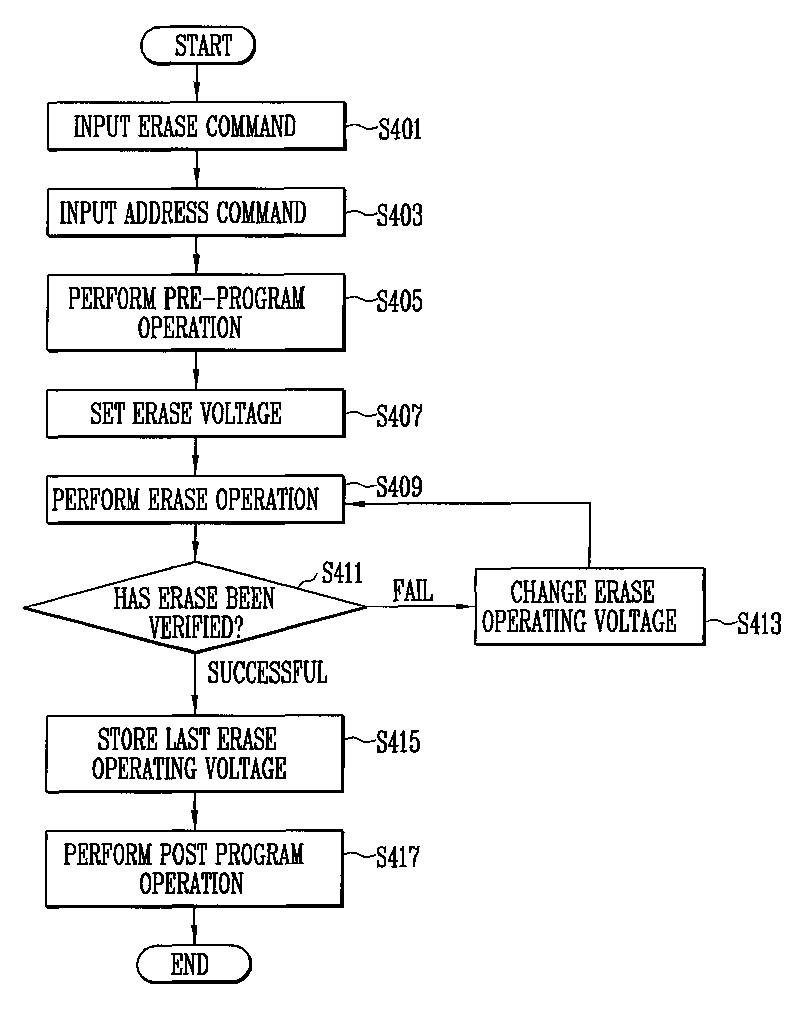
[0021]Specific embodiments according to the present patent will be described with reference to the accompanying drawings.

[0022]Referring to FIG. 3, the flash memory device according to an embodiment of the present invention includes a memory cell array 310, a page buffer 320, a high voltage generator 330, an X decoder 340, a switching unit 350, a well bias generator 360 and a controller 370.

[0023]The memory cell array 310 includes a plurality of memory cell blocks. Each of the memory cell blocks includes a plurality of cell strings (only one of the plurality of cell strings is illustrated for convenience). The cell string has a structure in which a drain select transistor DST, a plurality of memory cells C0 to Cn and a source select transistor SST are connected in series. The drain select transistor DST included in the cell string is connected to a corresponding bit line BLn, and the source select transistor SST is connected to a common source line CSL.

[0024]Meanwhile, the gates of ...


PUM


Abstract

An erase operating time can be shortened and an erase operating characteristic can be improved in a flash memory device. The flash memory device includes a plurality of memory cell blocks, an operating voltage generator and a controller. Each of the plurality of memory cell blocks includes memory cells connected to a plurality of word lines. A voltage generator is configured to apply an erase voltage to a memory cell block selected for an erase operation, and change a level of the erase voltage if an attempt of the erase operation is not successful. A controller is configured to control the voltage generator to apply a first erase voltage to a memory cell block selected for an erase operation. The first erase voltage corresponds to a previous erase voltage that was used successfully in completing a previous erase operation. The first erase voltage is an erase voltage that is used in a first erase attempt for the erase operation.

Description

CROSS-REFERENCES TO RELATED APPLICATIONS[0001]The present application claims priority to Korean patent application number 10-2007-029616, filed on Mar. 27, 2007, which is incorporated by reference in its entirety.BACKGROUND OF THE INVENTION[0002]The present invention relates to flash memory devices and, more particularly, to an erase method in which an erase operating time can be shortened and an erase operating characteristic can be improved.[0003]Semiconductor memory devices include non-volatile memory devices whose data is not lost even if the supply of power is cut off. The non-volatile memory devices include the flash memory device. The flash memory device includes a NOR flash memory device and a NAND flash memory device. Of them, the NAND flash memory device includes a memory cell array with a plurality of memory cell blocks. An erase operation of the NAND flash memory device is performed on a memory-cell-block basis. In general, the erase operation of the NAND flash memory de...

Claims


Application Information

Patent Timeline
Patent Type & Authority Patents(United States)
IPC IPC(8): G11C16/16
CPCG11C16/0483G11C16/16G11C16/344G11C16/3445G11C16/08G11C16/30
Inventor LEE, HEE YOUL
Owner SK HYNIX INC