Precise delay measurement through combinatorial logic

a combinatorial logic and delay measurement technology, applied in the field of digital electronic circuits, can solve the problems of not always oscillating, ring oscillator approach, inability to measure directly, etc., and achieve the effect of facilitating precise measurement of on-chip delays, facilitating precise measurement of propagation delays, and increasing the accuracy of propagation delay measuremen

Inactive Publication Date: 2010-10-05
NASA
View PDF11 Cites 13 Cited by
  • Summary
  • Abstract
  • Description
  • Claims
  • Application Information

AI Technical Summary

Benefits of technology

[0023]It is a more specific object to provide a built-in self-test (BIST) for FPGA propagation delay that embeds a pulse generator on the FPGA chip for propagating a pulse train through groupings of LUTs, and a pulse width measurement circuit (likewise on-chip) to measure the pulse width of the generated pulse through the delay chain, the pulse width representing the delay through the delay chain without any I/O delays, so that a determination of the propagation delay can be made very accurately.
[0024]It is still another object to provide a BIST architecture and test method as described above that uses an additional asynchronous clock autonomous from a main clock to increase the accuracy of the measurement of propagation delay.
[0025]In accordance with the foregoing objects, the present invention is a circuit that facilitates precise measurement of on-chip delays for FPGAs for reliability studies. The circuit incorporates an on-chip pulse generator, and on-chip pulse measurement circuitry programmed into a conventional semiconductor FPGA device to act as a performance monitor to measure the duration of a generated pulse through...

Problems solved by technology

The above-noted test procedure is problematic with FPGAs because many of the signal paths internal to the chip are not accessible via input and output pins, and therefore cannot be measur...

Method used


Image

  • Precise delay measurement through combinatorial logic
  • Precise delay measurement through combinatorial logic
  • Precise delay measurement through combinatorial logic

Examples


Embodiment Construction

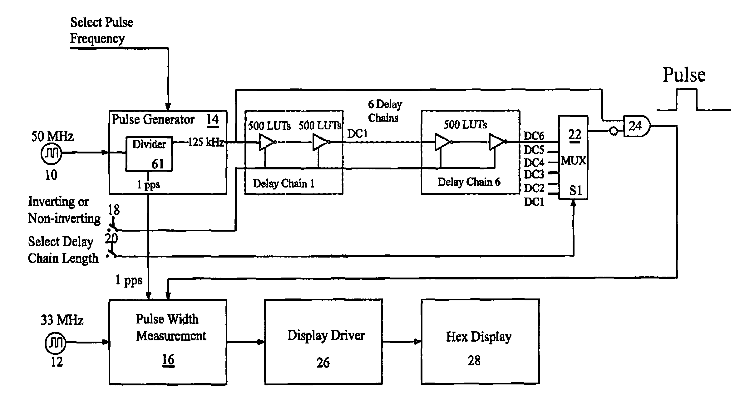
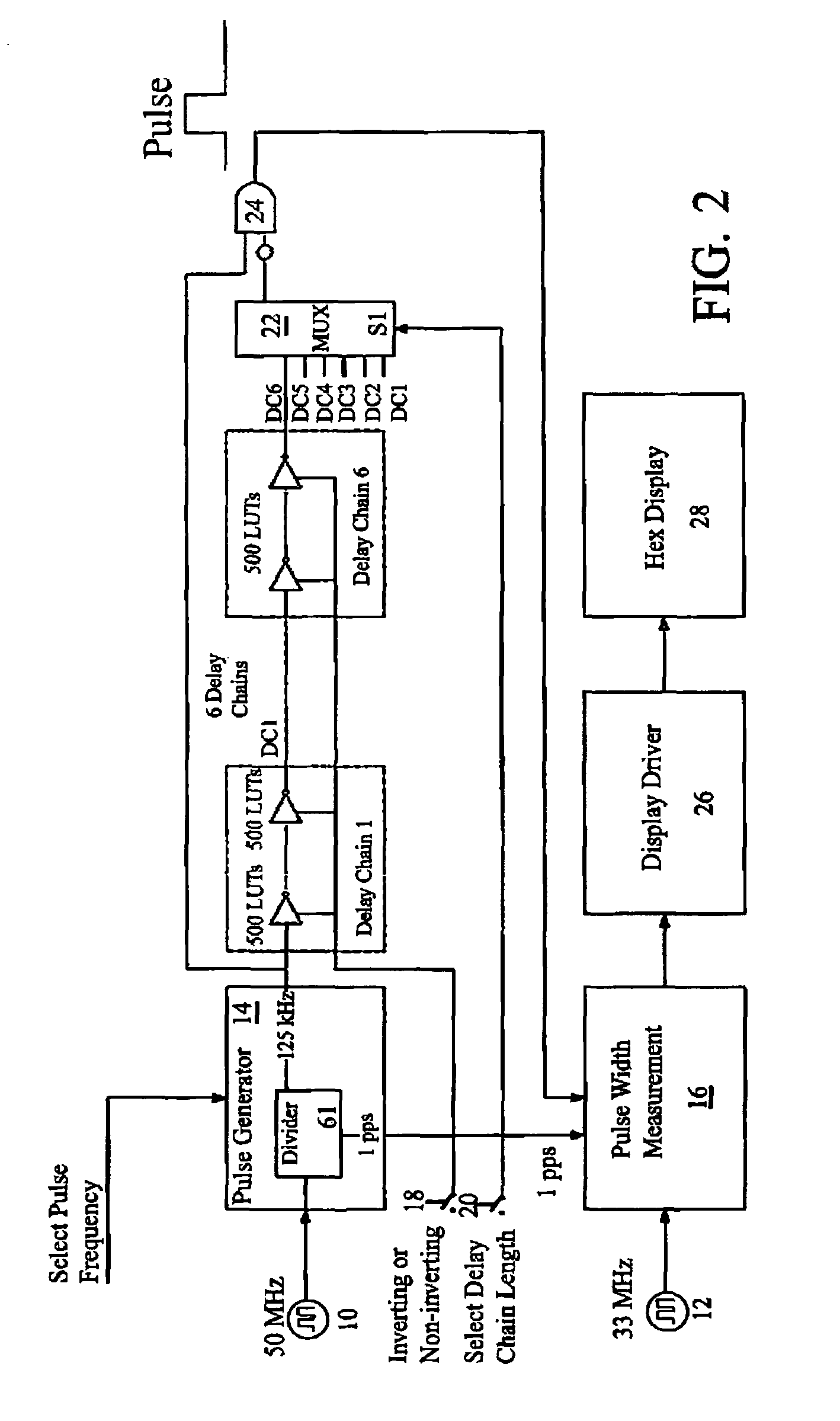
[0034]The present invention is a BIST test architecture and method for precise measurement of on-chip delays for FPGAs to be used in reliability studies. The architecture incorporates an on-chip pulse generator and on-chip pulse measurement circuitry to measure the duration of a generated pulse through one or more groups of LUTS (the “LUT delay chain”) also on-chip. The measured pulse width represents the delay through the LUT delay chain under test. Since the pulse is generated on-chip there are no significant I / O delays, and the delay measurements can be made very accurately. The on-chip pulse width measurement circuit uses an additional asynchronous clock autonomous from a main clock to greatly improve the sampling rate and resulting accuracy. The on-chip pulse measurement circuitry is configured to measure the pulse width of the output pulse, which is then converted to a hex value using state machines, counters and lookup tables. The result is displayed on a multidigit hex displ...


PUM


Abstract

A high resolution circuit and method for facilitating precise measurement of on-chip delays for FPGAs for reliability studies. The circuit embeds a pulse generator on an FPGA chip having one or more groups of LUTS (the “LUT delay chain”), also on-chip. The circuit also embeds a pulse width measurement circuit on-chip, and measures the duration of the generated pulse through the delay chain. The pulse width of the output pulse represents the delay through the delay chain without any I/O delay. The pulse width measurement circuit uses an additional asynchronous clock autonomous from the main clock and the FPGA propagation delay can be displayed on a hex display continuously for testing purposes.

Description

STATEMENT OF GOVERNMENT INTEREST[0001]The invention described hereunder was made in the performance of work under a NASA contract, and is subject to the provisions of Public Law #96-517 (35 U.S.C. 202) in which the Contractor has elected not to retain title.BACKGROUND OF THE INVENTION[0002]1. Field of the Invention[0003]The present invention relates to digital electronic circuits and, more particularly, to a method and system for measuring on-chip delays for Field Programmable Gate Arrays (FPGAs) for reliability testing.[0004]2. Description of Prior Art[0005]A Field Programmable Gate Array or FPGA is a semiconductor device containing programmable logic components that can be programmed to duplicate the functionality of basic logic gates such as AND, OR, XOR, NOT or more complex combinatorial functions such as decoders or simple math functions. The FPGA also contains sequential logic in the form of configurable flip / flops. Many FPGAs also include memory elements such as RAMs.[0006]An...

Claims


Application Information

Patent Timeline
IPC IPC(8): H03K19/00G06F17/00
CPCG01R31/3016G01R31/318519H03K19/17764H03K19/177
Inventor BURKE, GARY R.CHEN, YUANSHELDON, DOUGLAS J.
Owner NASA
Why Eureka
Try Eureka