Method of manufacturing semiconductor device having trench-gate transistor

a manufacturing method and trench-gate technology, applied in the direction of semiconductor devices, basic electric elements, electrical appliances, etc., can solve the problems of disadvantageous increase of sub-threshold current, and increase junction leakage, so as to improve the uniform thickness and width of the thin film part, the effect of reducing the characteristic irregularities of a plurality of transistors

Active Publication Date: 2010-10-19
MICRON TECH INC
View PDF14 Cites 6 Cited by
  • Summary
  • Abstract
  • Description
  • Claims
  • Application Information

AI Technical Summary

Benefits of technology

[0006]Therefore, it is an object of the present invention to provide a method of manufacturing a semiconductor device having a trench-gate transistor which can suppress junction leakage current, reduce power supply voltage and reduce characteristic irregularities among a plurality of transistors.
[0015]As described above, according to the present invention, the upper end of the first insulating film for forming the STI region is made to include the shoulder part almost perpendicular to the semiconductor substrate, and the shoulder part is covered with the second and third insulating films. By doing so, in the dry etching for forming the opening in the fourth insulating film, the shoulder part of the first insulating film is protected. Therefore, the shoulder part of the first insulating film is not chipped. When the gate trench is formed by etching the semiconductor substrate using the shoulder part as a mask, a part of the semiconductor substrate left as a thin film part between the gate trench and the STI region can be prevented from being tapered on the gate trench side. It is thereby possible to improve uniformity in thickness and width of the thin film part to serve as the channel region of each transistor. Accordingly, characteristic irregularities among a plurality of transistors can be reduced.

Problems solved by technology

However, if the gate length is smaller, then the short channel effect of the transistor disadvantageously becomes more conspicuous, and sub-threshold current is disadvantageously increased.
Furthermore, if substrate concentration is increased to suppress the short channel effect and the increase of the sub-threshold current, junction leakage increases.
Due to this, the DRAM is confronted with a serious problem of deterioration in refresh characteristics.
However, the conventional trench-gate transistor has the following problems.

Method used


Image

  • Method of manufacturing semiconductor device having trench-gate transistor
  • Method of manufacturing semiconductor device having trench-gate transistor
  • Method of manufacturing semiconductor device having trench-gate transistor

Examples


Embodiment Construction

[0038]To improve the semiconductor device including the trench-gate transistor, the present inventor was dedicated to various studies and considerations before the present invention is invented. Consequently, a related art proposed by the present inventor will be firstly explained below.

[0039]FIGS. 18A and 18B are views for explaining a structure of a semiconductor device according to the related art. FIG. 18A is a generally plan view and FIG. 18B is a generally cross-sectional view taken along a line X-X′ shown in FIG. 18A.

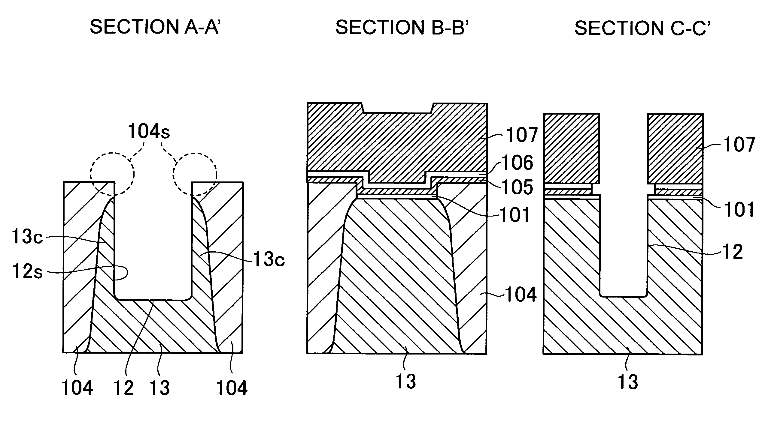
[0040]As shown in FIG. 18A, gate trenches 202 are formed in one direction to cross an active region 201 surrounded by an STI (Shallow Trench Isolation) region 200. As shown in FIG. 18B, gate insulating films 203 are formed on side surfaces of each of the gate trenches 202, an insulating film 204 thicker than the gate insulating films 203 is formed on a bottom of each of the gate trenches 202, and a gate electrode 205 is formed in each gate trench 202. A part 206c...


PUM


Abstract

A method of manufacturing a semiconductor device includes: a first step of forming an STI region and an active region surrounded by the STI region on a semiconductor substrate; a second step of forming a protection film protecting a shoulder part of the STI region in a boundary between the active region and the STI region; a third step of forming a gate trench in the active region so as to leave a part of the semiconductor substrate located between a side surface of the STI region and a side surface of the gate trench;a fourth step of forming a gate insulating film on the side surface of the gate trench; a fifth step of forming a gate electrode, at least a part of the gate electrode being buried in the gate trench; and a sixth step of forming a source region and a drain region in regions located on both sides of the gate trench in an extension direction of the gate trench, respectively, so that the part of the semiconductor substrate functions as a channel region.

Description

TECHNICAL FIELD[0001]The present invention relates to a semiconductor device manufacturing method, and particularly relates to a method of manufacturing a semiconductor device including a trench-gate transistor.BACKGROUND OF THE INVENTION[0002]In recent years, following downsizing of a memory cell in a DRAM (Dynamic Random Access Memory), a gate length of a memory cell transistor is inevitably reduced. However, if the gate length is smaller, then the short channel effect of the transistor disadvantageously becomes more conspicuous, and sub-threshold current is disadvantageously increased. Furthermore, if substrate concentration is increased to suppress the short channel effect and the increase of the sub-threshold current, junction leakage increases. Due to this, the DRAM is confronted with a serious problem of deterioration in refresh characteristics.[0003]To avoid the problem, attention is paid to a so-called trench-gate transistor (also called as “recess-channel transistor”) conf...

Claims


Application Information

Patent Timeline
Patent Type & Authority Patents(United States)
IPC IPC(8): H01L21/8234
CPCH01L21/76232H01L27/10876H01L27/10879H01L29/66795H01L29/7853H10B12/056H10B12/053
Inventor KUJIRAI, HIROSHI
Owner MICRON TECH INC
Why Eureka
Try Eureka