Method of separating semiconductor dies

Active Publication Date: 2010-11-09
SEMILEDS OPTOELECTRONICS CO LTD
View PDF9 Cites 6 Cited by
  • Summary
  • Abstract
  • Description
  • Claims
  • Application Information

AI Technical Summary

Benefits of technology

[0008]Embodiments of the present invention generally provide techniques and structures useful for separating multiple semiconductor dies present on a wafer. The methods described herein may provide a working semiconductor structure with enough th

Problems solved by technology

Cutting through a thicker substrate generally takes more time and energy than cutting through a thinner substrate and is sometimes not possible if the substrate comprises thick metal layers that cause gumming of the saw blade or requires excessive laser energy, thereby damaging the die and lowering t

Method used


Image

  • Method of separating semiconductor dies
  • Method of separating semiconductor dies
  • Method of separating semiconductor dies

Examples


Embodiment Construction

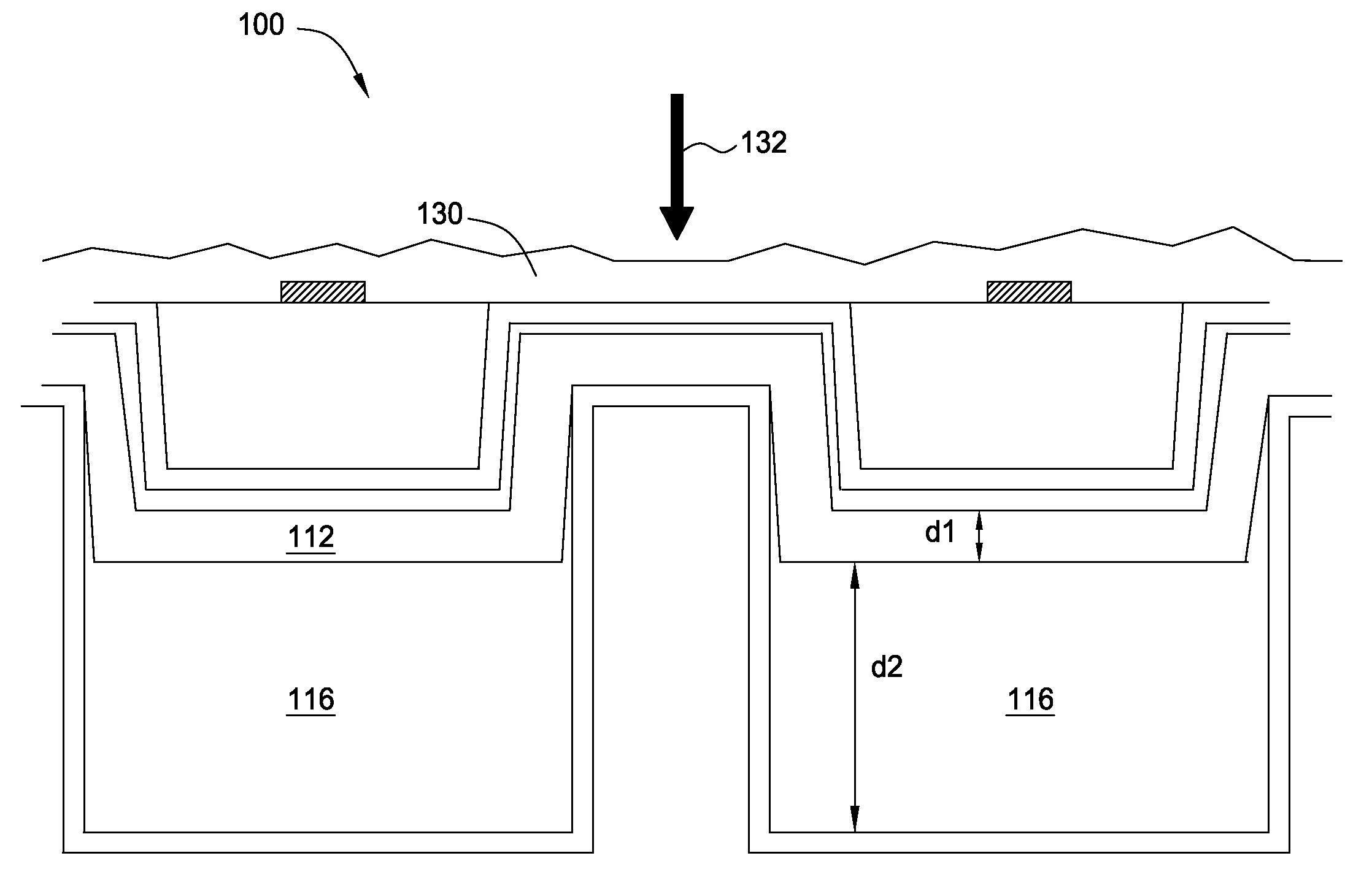
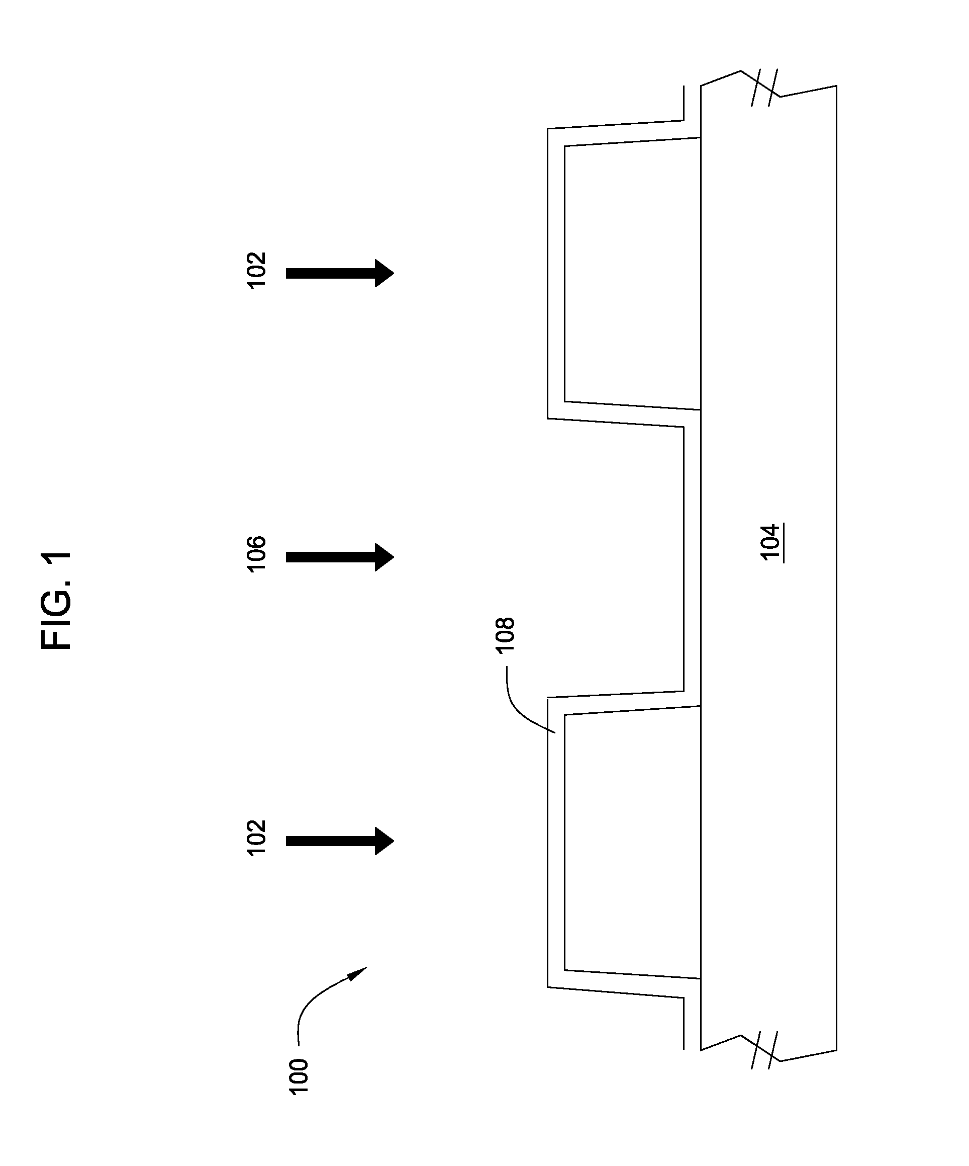
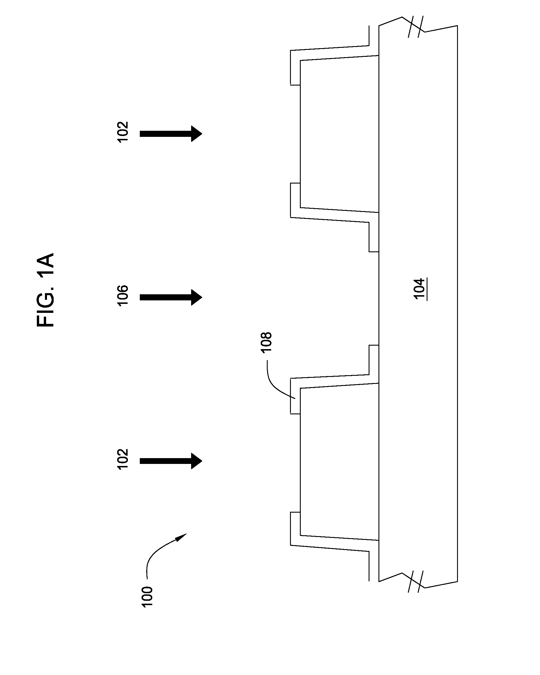
[0035]Embodiments of the present invention provide techniques and structures useful for separating multiple semiconductor dies present on a wafer. This method may be applied to any semiconductor wafer with multiple dies, and the case of separating multiple vertical light-emitting diode (VLED) dies is provided as a particular, but not limiting, example. In the figures that follow, only two dies are shown, but this is representative of multiple dies on the entire wafer.

An Exemplary Die Separation Method

[0036]Referring now to FIG. 1, a generic multilayered semiconductor structure 100 may be provided with two or more different dies 102 disposed on a substrate 104 and separated by a street section, or simply “the street”106. The dies may have been epitaxially deposited on the substrate, which may be composed of any suitable material, such as SiO2, sapphire, GaAs, InP, InGaAsP, Si, ZnO, or AlN. A passivation layer 108 may be deposited on the dies 102. A portion of the passivation layer ma...


PUM


Abstract

A method for the separation of multiple dies during semiconductor fabrication is described. On an upper surface of a semiconductor wafer containing multiple dies, a seed metal layer may be used to grow hard metal layers above it for handling. Metal may be plated above these metal layers everywhere except where a block of stop electroplating (EP) material exists. The stop EP material may be obliterated, and a barrier layer may be formed above the entire remaining structure. The substrate may be removed, and the individual dies may have any desired bonding pads and/or patterned circuitry added to the semiconductor surface. The remerged hard metal after laser cutting and heating should be strong enough for handling. Tape may be added to the wafer, and a breaker may be used to break the dies apart. The resulting structure may be flipped over, and the tape may be expanded to separate the individual dies.

Description

CROSS-REFERENCE TO RELATED APPLICATIONS[0001]This application claims benefit of U.S. Provisional Application Ser. No. 60 / 821,608 filed Aug. 7, 2006, which is herein incorporated by reference.BACKGROUND OF THE INVENTION[0002]1. Field of the Invention[0003]Embodiments of the present invention generally relate to a method of semiconductor fabrication, and more particularly, to a method of separating multiple semiconductor dies.[0004]2. Description of the Related Art[0005]A wide variety of electronic devices, ranging from microprocessors to light-emitting diode (LED) structures, are typically formed in relatively large numbers as die on semiconductor wafer substrates. After formation, the devices must be separated for final packaging, typically via mechanical saw, “scribing and break,” or laser. Conventionally, the backside of the wafer substrates is flat, and in order to separate the die, one must cut through a relatively thick substrate. Cutting through a thicker substrate generally t...

Claims


Application Information

Patent Timeline
IPC IPC(8): H01L21/301
CPCH01L21/78H01L33/0095H01L33/0079H01L33/0093
Inventor CHU, JIUNN-YICHENG, CHAO-CHENCHU, CHEN-FUDOAN, TRUNG TRI
Owner SEMILEDS OPTOELECTRONICS CO LTD
Why Eureka
Try Eureka