Method for manufacturing a nitride semiconductor laser element and a nitride semiconductor laser element

a laser element and semiconductor technology, applied in the field of manufacturing a nitride semiconductor laser element, can solve the problems of affecting the yield of the desired cavity length, difficult to obtain a sufficiently stable yield, and the distorted cleavage plane of the intended position, so as to improve the yield and prevent the effect of the start-up voltage decrease and good current and voltage characteristics

Active Publication Date: 2010-11-23
NICHIA CORP
View PDF9 Cites 4 Cited by
  • Summary
  • Abstract
  • Description
  • Claims
  • Application Information

AI Technical Summary

Benefits of technology

[0010]An object is to provide a method for manufacturing a nitride semiconductor laser element with which the cleavage of a cavity end face can be performed at the intended location, yield is improved, and a laser element of consistent quality can be manufactured efficiently.
[0011]Another object is to provide a nitride semiconductor laser element in which a decrease in start-up voltage can be prevented, good current and voltage characteristics as well as consistent quality can be obtained.
[0019]With the method of the present invention for manufacturing a nitride semiconductor laser element, an island layer is formed so as to sandwich an intended division location, the effect being that the cavity end face can be formed by dividing the substrate and the laminate at the desired location, which improves the yield.
[0020]Also, with the nitride semiconductor laser element of the present invention, a decrease in start-up voltage can be prevented, good current and voltage characteristics as well as consistent quality are obtained.

Problems solved by technology

However, even when the cleavage of a cavity end face is performed substantially perpendicular to these grooves, the effect of the dislocation density, crystal defects, etc., within the nitride semiconductor layer or substrate can cause the cleavage plane to be distorted from its intended position, making it difficult to obtain a sufficiently stable yield.
Consequently, if the primary cleavage is distorted from its intended position, a laser element of the desired cavity length will not be obtained, and this greatly affects the characteristics.
Also, when the division is made where the electrodes are formed, the electrodes may droop down to the cavity end face, and this adversely and markedly affects the characteristics.
Furthermore, it is difficult to divide the semiconductor layer bars into chips, and this greatly affects the yield.
When a laser element is produced from a nitride semiconductor, a problem is that leakage caused by these dislocations and crystal defects can lower the voltage in the minute electric current region and result in poor current and voltage characteristics.
If the start-up voltage is low, this leads to problems such as a shorter element service life and poor electrostatic discharge.

Method used


Image

  • Method for manufacturing a nitride semiconductor laser element and a nitride semiconductor laser element
  • Method for manufacturing a nitride semiconductor laser element and a nitride semiconductor laser element
  • Method for manufacturing a nitride semiconductor laser element and a nitride semiconductor laser element

Examples


example 1

[0160]A method for manufacturing a laser element of this Example is explained by the following.

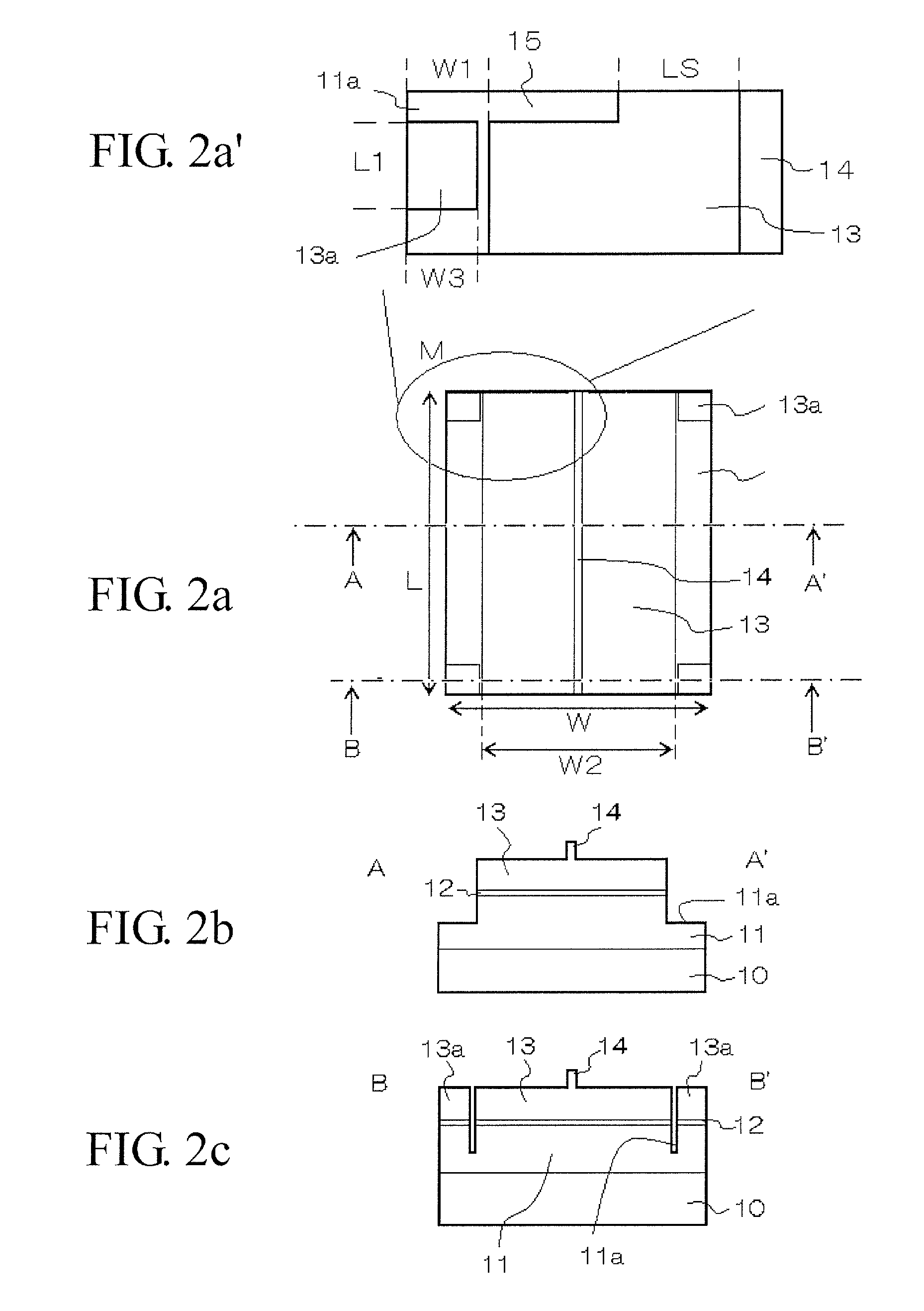
[0161]First, an n-GaN substrate is set in a reaction vessel of the MOVPE apparatus. In the reaction vessel, a first buffer layer composed of n-Al0.02Ga0.98N doped with Si at 1×10¹⁸ / cm3 is grown on the GaN substrate using trimethyl aluminum (TMA), trimethyl gallium (TMG) and ammonia (NH3) as the raw material gas with a silane gas for an impurity gas. After that, a second buffer layer composed of n-In0.04Ga0.96N doped with Si at 1×10¹⁸ / cm3 is grown using trimethylindium (TMI), TMG and NH3 as the raw material gas with a silane gas for an impurity gas.

[0162]An n-side clad layer composed of Al0.11Ga0.89N doped with Si at 1×10¹⁸ / cm3 is grown using TMG, TMA and NH3.

[0163]Next, n-side wave guide layer composed of undoped Al0.06Ga0.94N is grown.

[0164]The temperature is set to 950° C., a barrier layer composed of Al0.15Ga0.85N doped with Si at 1×10¹⁹ / cm3 is grown using TMA, TMG and NH3. The silane g...

example 2

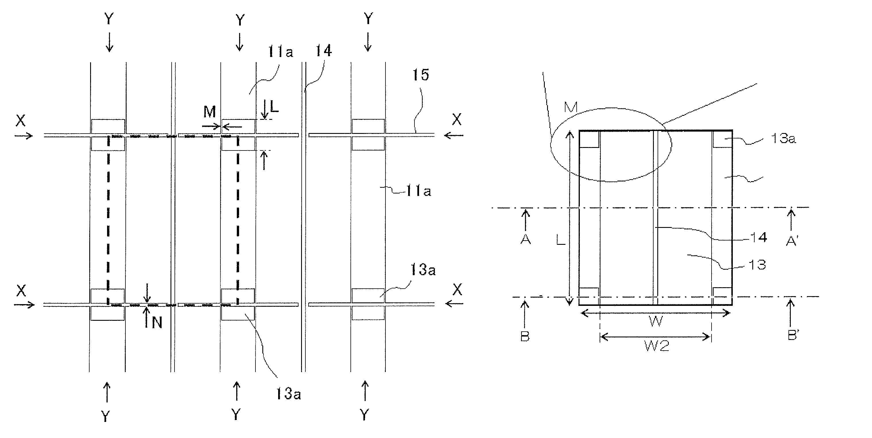
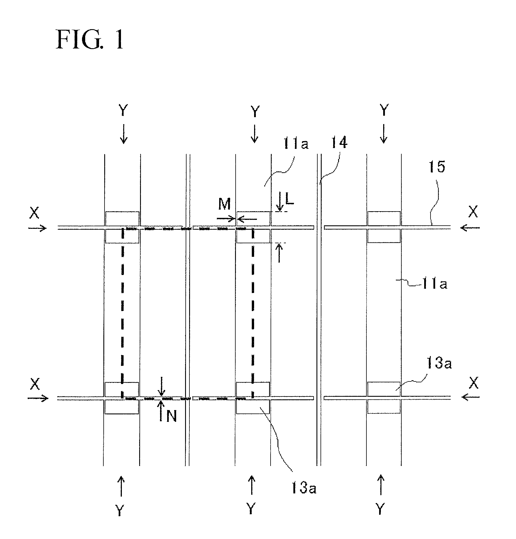
[0184]A semiconductor laser chip is produced by substantially the same method as in Example 1, except that n-type GaN is used, a substrate having a first region of the (0001) plane and a second region of the (000-1) plane, respectively, a low dislocation density region and a high dislocation density region is used, the width of the exposed regions is changed in an alternating pattern, and the widths of the exposed region and the island layer are varied in the cavity end face.

[0185]As shown in FIG. 6, the laser element of this Example comprised an exposed region 11a and an exposed region 21a, which respectively have widths of about 70 μm and about 30 μm, and the widths of island layers 13b and 21b near the cavity end face are respectively about 160 μm and about 120 μm.

[0186]As shown in FIGS. 7a to 7d, the laser element obtained by this manufacturing method is such that the island layers 13a and 21b are formed with varying widths in the cavity direction. Since the island layers are di...

example 3

[0188]As shown in FIG. 9, a V-shaped laser scribed groove is formed as a second auxiliary groove 16, from the p-type contact layer to the substrate, at a focal distance of just focus ±10 μm, a feed rate of 1 to 200 μm / sec, and an output of 0.1 to 10 W, in a direction perpendicular to the cavity direction, after p-side ohmic electrode and an n-side ohmic electrode are formed, but before the cavity end face is produced. The maximum depth of the laser scribed groove in this case is about 25 μm, and the width of the groove on the p-type contact layer surface (the width of the opening of the V-groove) is about 5 μm. The length of the second auxiliary groove 16 in the island layer 13b is 140 μm, and the length of the second auxiliary groove in the island layer 21b is 100 μm.

[0189]After this, an acetic acid solution is used to ultrasonically wash the interior and surface of the laser scribed groove, and any scattered material, etc., adhering thereto is removed.

[0190]A laser element is then...


PUM

PropertyMeasurementUnit
off angleaaaaaaaaaa
off angleaaaaaaaaaa
thicknessaaaaaaaaaa

Abstract

A method for manufacturing a nitride semiconductor laser element, which has over a substrate a laminate including an element region constituting a cavity, an island layer separated from the element region, an exposed region separating the element region from the island layer, and an auxiliary groove provided along an end face of the cavity, and with which the cavity end face is obtained by dividing the laminate and the substrate along the first auxiliary groove, the method comprises a step of: forming the laminate over the substrate; removing part of the laminate to separate the laminate into the element region and the island layer and to form the exposed region provided continuously in the cavity direction of the nitride semiconductor laser element; forming the first auxiliary groove so as to be adjacent to the island layer; and dividing so that the island layer is disposed in a corner of the nitride semiconductor laser element to obtain a nitride semiconductor laser element.

Description

BACKGROUND OF THE INVENTION[0001]1. Field of the Invention[0002]This invention relates to a method for manufacturing a nitride semiconductor laser element and a nitride semiconductor laser element.[0003]2. Background Information[0004]There is growing demand for semiconductor laser elements in which a compound semiconductor, for example, nitride semiconductors expressed by the general formula InxAlyGa1−x−yN (0≦x, 0≦y, 0≦x+y≦1) are used, in a wide variety of applications, such as in optical disk systems capable of recording and reproducing large volumes of information at high density (such as a next-generation DVD), or in electronic devices such as personal computers. Therefore, considerable research has been devoted to using nitride semiconductors to manufacture semiconductor laser elements with good reproducibility while maintaining stable characteristics.[0005]For example, a method in which grooves that extend in a cavity direction of a laser element and is formed from the upper fa...

Claims


Application Information

Patent Timeline
Patent Type & Authority Patents(United States)
IPC IPC(8): H01S5/183
CPCB82Y20/00H01S5/0201H01S5/34333H01S5/0202H01S5/22H01S2301/173
Inventor MASUI, SHINGO
Owner NICHIA CORP
Why Eureka
Try Eureka