
Organic light emitting diode display

a light-emitting diode and organic technology, applied in the field of organic light-emitting diodes (“ oled ”) display, can solve the problems of lcd response speed and viewing angle, and achieve the effect of improving contrast ratio and increasing the number of manufacturing processes

Active Publication Date: 2010-11-30
SAMSUNG DISPLAY CO LTD
View PDF25 Cites 4 Cited by
  • Summary
  • Abstract
  • Description
  • Claims
  • Application Information

AI Technical Summary

Benefits of technology

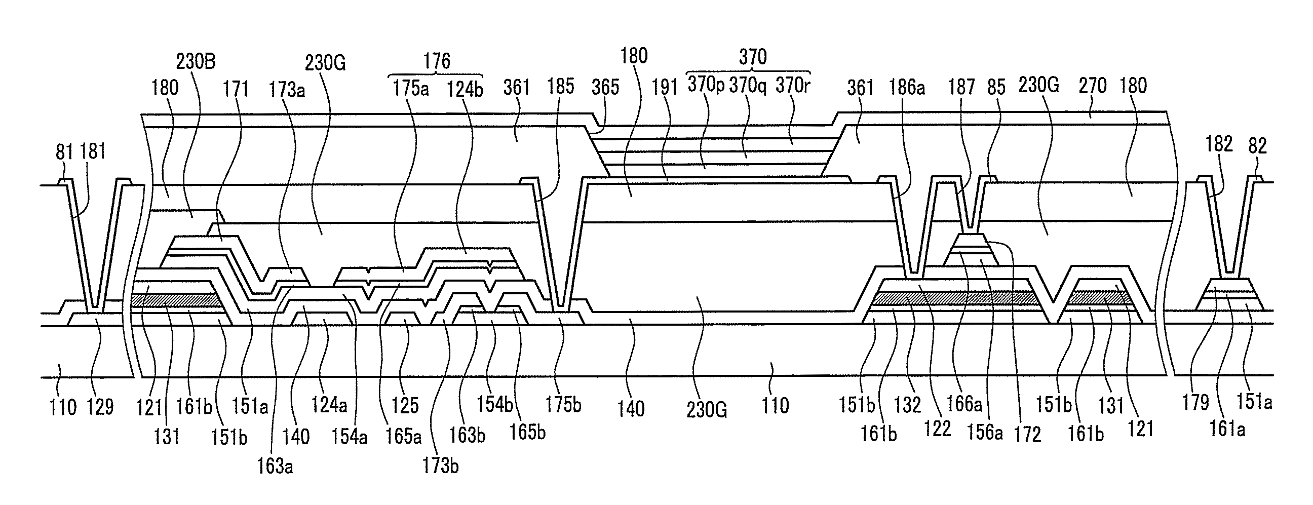
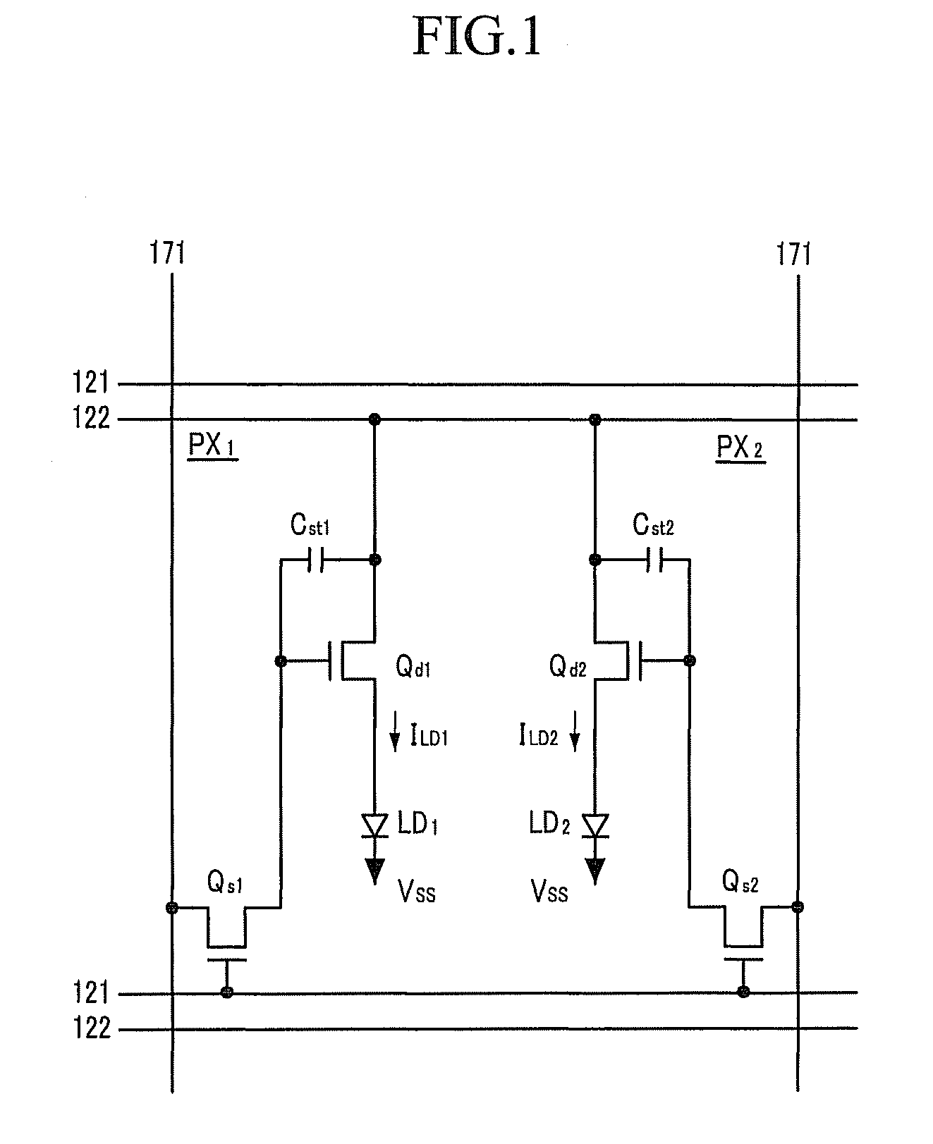
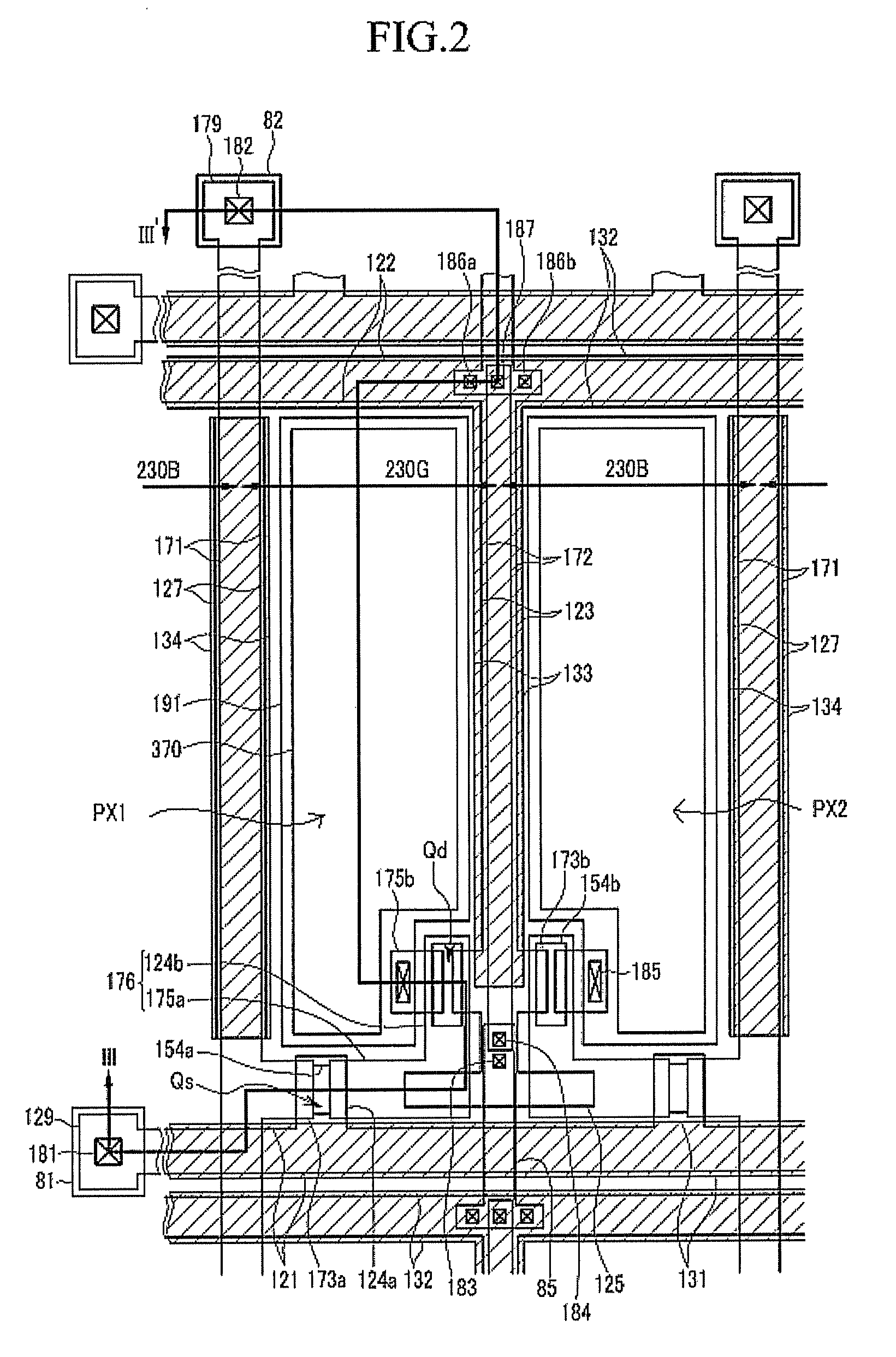
The present invention provides an organic light emitting device display that can simultaneously meet the requirements of a switching thin film transistor and a driving thin film transistor without increasing the number of manufacturing processes. Additionally, the invention provides an OLED display with an improved contrast ratio. The invention also includes a light blocking member, a switching control electrode, a first amorphous semiconductor, a second amorphous semiconductor, a second crystalline semiconductor, an etch stopper, a color filter, and a light emitting member. The invention also includes a first pixel and a second pixel with a driving voltage line and a light blocking member. The technical effects of the invention include improved manufacturing efficiency, improved contrast ratio, and improved performance of the organic light emitting device display.

Problems solved by technology

Also, the LCD has problems in terms of response speed and viewing angle.

Method used


Image

  • Organic light emitting diode display
  • Organic light emitting diode display
  • Organic light emitting diode display

Examples


Embodiment Construction

[0070]The invention now will be described more fully hereinafter with reference to the accompanying drawings, in which embodiments of the invention are shown. This invention may, however, be embodied in many different forms and should not be construed as limited to the embodiments set forth herein. Rather, these embodiments are provided so that this disclosure will be thorough and complete, and will fully convey the scope of the invention to those skilled in the art. Like reference numerals refer to like elements throughout.

[0071]It will be understood that when an element is referred to as being “on” another element, it can be directly on the other element or intervening elements may be present therebetween. In contrast, when an element is referred to as being “directly on” another element, there are no intervening elements present. Further, it will be understood that when a first element is referred to as being “on” a second element, the first element may be above or below the seco...


PUM


Abstract

An organic light emitting diode (“OLED”) display includes a substrate, a gate line, a data line, a driving voltage line, a light blocking member, a switching thin film transistor (“TFT”), a driving TFT, and an OLED, wherein the driving voltage line includes a portion parallel to at least one of the gate line and the data line, the light blocking member is formed under at least one of the gate line, the data line, and the driving voltage line, the switching TFT is connected to the gate line and the data line and includes an amorphous semiconductor, the driving TFT is connected to the switching TFT and includes a polycrystalline semiconductor, and the OLED is connected to the driving TFT.

Description

[0001]This application claims priority to Korean Patent Application No. 10-2006-0055856, filed on Jun. 21, 2006, and all the benefits accruing therefrom under 35 U.S.C. §119, the contents of which in its entirety are herein incorporated by reference.BACKGROUND OF THE INVENTION[0002](a) Field of the Invention[0003]The present invention relates to an organic light emitting diode (“OLED”) display and a method for manufacturing the same.[0004](b) Description of the Related Art[0005]Recently, monitors and television sets have been required to be thinner and lighter. In order to satisfy such requirements, liquid crystal displays (“LCD”) have replaced cathode ray tube (“CRT”) displays.[0006]However, an LCD requires an additional backlight because the LCD is a passive light emitting device. Also, the LCD has problems in terms of response speed and viewing angle.[0007]In order to overcome the problems of the LCD, an organic light emitting diode (“OLED”) display has being receiving attention....

Claims


Application Information

Patent Timeline
Patent Type & Authority Patents(United States)
IPC IPC(8): H01L51/00H10K99/00
CPCH01L27/1214H01L27/1288H01L27/3244H10K59/12H05B33/00H05B33/10
Inventor CHOI, JOON-HOOHUH, JONG-MOOGOH, JOON-CHULPARK, SEUNG-KYUJUNG, KWANG-CHUL
Owner SAMSUNG DISPLAY CO LTD
Learn More