

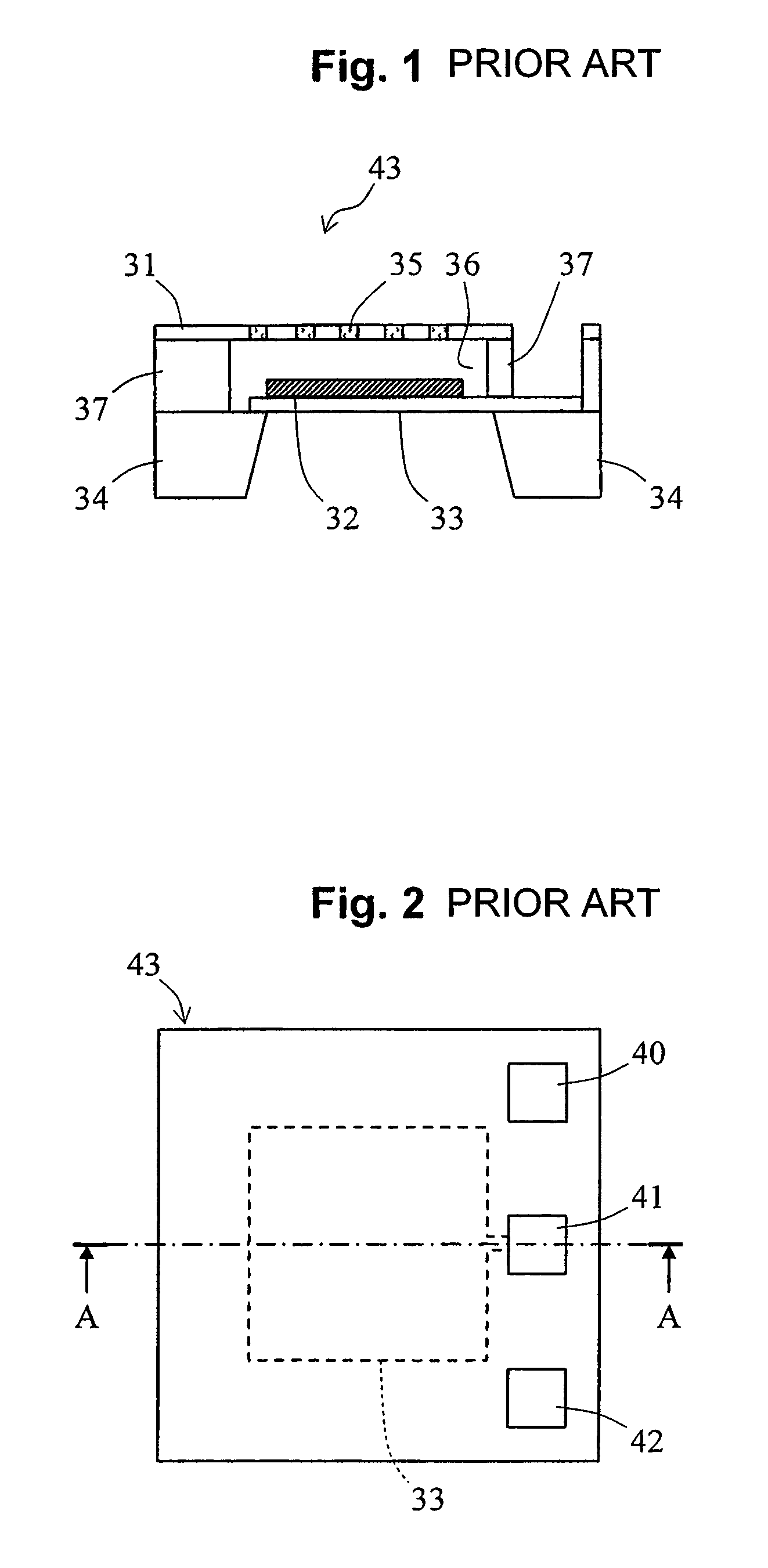
Method of fabricating an ultra-small condenser microphone
a condenser microphone and ultra-small technology, applied in the direction of electrical transducers, semiconductor devices, electrical apparatus, etc., can solve the problems of limited productivity, low throughput, and high sensitivity of partially fabricated mems microphone chips, so as to improve positioning accuracy, high speed, and low throughput
- Summary
- Abstract
- Description
- Claims
- Application Information
AI Technical Summary
Benefits of technology
Problems solved by technology
Method used
Image

Examples
first embodiment
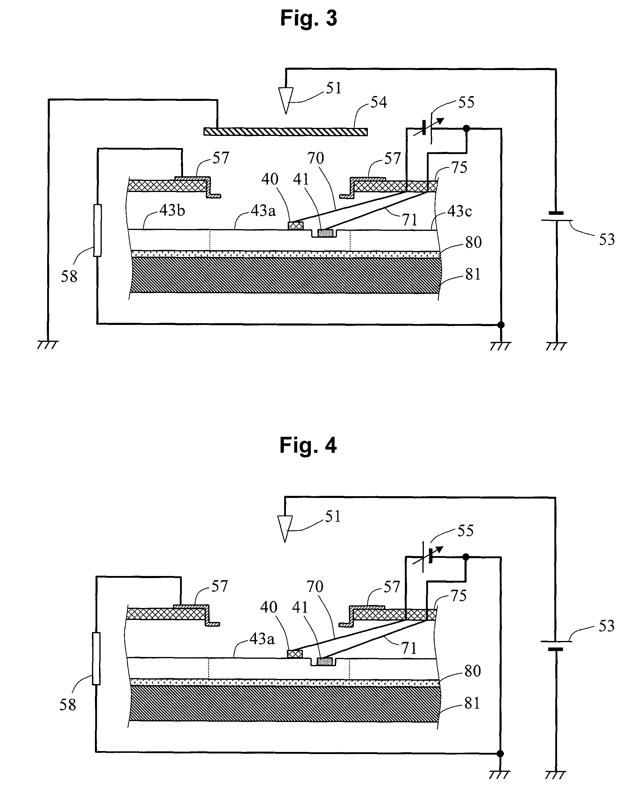
[0046]FIG. 3 is a schematic cross-sectional view showing a principal part of a structure of an electretization apparatus used for an electretization process of an ultra-small condenser microphone in accordance with a first embodiment of the present invention. In the electretization apparatus in FIG. 3, a plurality of ultra-small condenser microphones (MEMS microphones), which is formed on a same semiconductor substrate, in a state of a substrate not being diced is electretized. The electretization to a MEMS microphone chip is performed by irradiating a single MEMS microphone chip formed on the semiconductor substrate with ions resulting from a corona discharge of a single needle electrode in this apparatus.
[0047]As shown in FIG. 3, the electretization apparatus in this embodiment is provided with a stage 81 on which a semiconductor substrate having a plurality of MEMS microphone chips 43 (only MEMS microphone chips 43a, 43b and 43c are shown in FIG. 3) is disposed. The stage 81 has ...
second embodiment
[0066]FIG. 6 is a schematic cross-sectional view showing a principal part of a structure of an electretization apparatus used for an electretization process of an ultra-small condenser microphone in accordance with a second embodiment of the present invention. The electretization apparatus shown in FIG. 6 has a structure that a chip 43 to be electretized is electretized and simultaneously an amount of deposited charges of a MEMS microphone chip 44 which has been completed the electretization (hereinafter referred to as the electretized chip 44) on the same semiconductor substrate is inspected. In FIG. 6, a MEMS microphone chip 43 locates several pieces left-hand from a MEMS microphone chip 43a as a reference chip on the semiconductor substrate, that is not particularly limited, is regarded as the electretized chip 44. In FIG. 6, components having the same function as those in FIG. 3 are referred to by the same reference numbers.
[0067]As shown in FIG. 6, in the electretization appara...
third embodiment
[0081]In the first and the second embodiments, the electretization is performed by a corona discharge using a needle electrode. The electretization, however, can be performed using a linear electrode in stead of the needle electrode. Thus, the electretization that is performed by a corona discharge using a linear discharge electrode will be discussed in this embodiment.
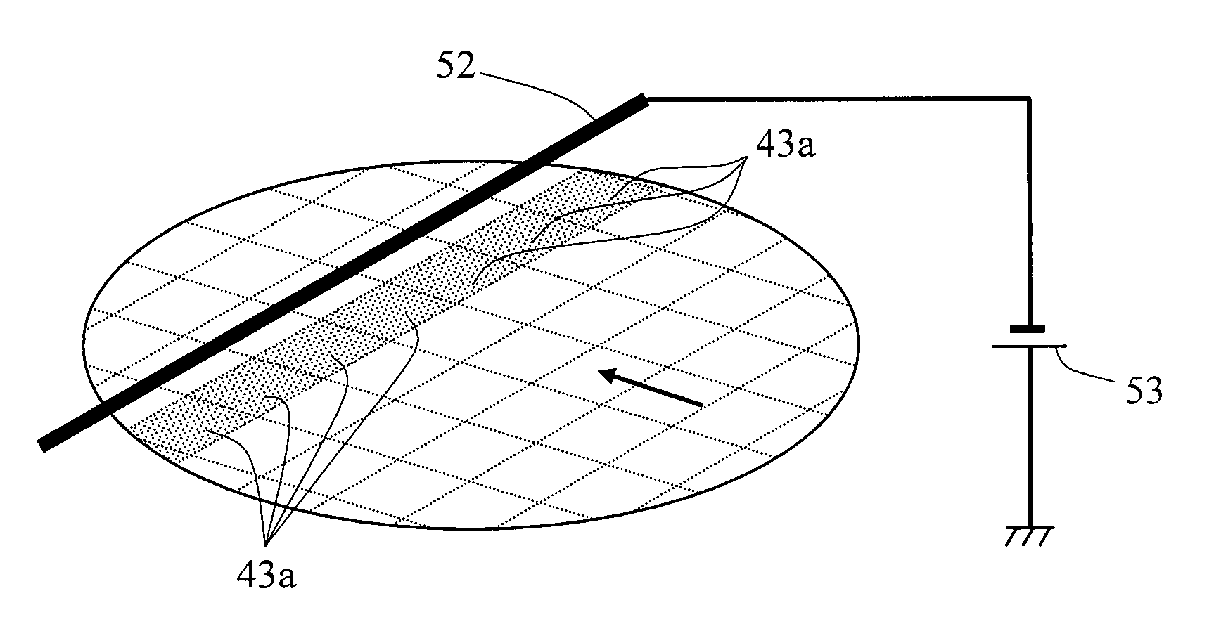
[0082]FIG. 9 is a schematic enlarged view showing a principal part of an electretization apparatus used in an electretization process of an ultra-small condenser microphone in accordance with a third embodiment. The electretization apparatus in FIG. 9 is provided with a wire electrode 52 (discharge electrode) which is a linear-formed in stead of the needle electrode 51 in the electretization apparatus described in the first embodiment. The wire electrode 52 simultaneously irradiates a plurality of MEMS microphone chips 43a to be electretized arranged linearly in one direction with ions resulting from a corona discharg...
PUM
| Property | Measurement | Unit |
|---|---|---|
| voltage | aaaaa | aaaaa |
| conducting state | aaaaa | aaaaa |
| non-conducting | aaaaa | aaaaa |
Abstract
Description
Claims
Application Information