Light emitting device and method of manufacturing the same

a technology manufacturing method, which is applied in the direction of semiconductor device details, semiconductor/solid-state device details, electrical apparatus, etc., can solve the problems of inability to securely prone to pinholes and cracks, and inability to secure cover such a stepped part with insulating film, etc., to achieve enhanced reliability stable characteristics, and increase the yield of light emitting device

Inactive Publication Date: 2010-12-28
SONY CORP
View PDF29 Cites 10 Cited by
  • Summary
  • Abstract
  • Description
  • Claims
  • Application Information

AI Technical Summary

Benefits of technology

[0064]In the present invention, the second electrode is covered with an SOG layer. The SOG material layer serving as a kind of precursor (SOG layer precursor) for forming the SOG layer is liquid, and the second electrode can be covered with the SOG material layer by a coating method. Therefore, the second electrode can be assuredly covered with a continuous film free of grain boundaries, and generation of pinholes or cracks can be obviated. As a result, moisture (water) from the external atmosphere can be securely prevented from reaching the second electrode including silver (Ag) or ITO, whereby it is possible to securely obviate the problem that ion migration is generated or whiskers are formed in the second electrode, leading to deterioration of the second electrode and, hence, to deterioration of characteristics of the light emitting diode. Therefore, it is possible to contrive enhanced reliability of the light emitting device, to maintain stable characteristics even under severe environmental conditions, and to achieve an increase in the yield of the light emitting device.
[0065]Incidentally, when the first insulating layer is formed under the SOG layer and / or the second insulating layer is formed over the SOG layer, the reliability of the light emitting device can be enhanced more. In addition, since the under layer (substrate layer) inclusive of the second electrode can be covered by a coating method, the discontinuity of stepped parts can be compensated for by a smoothing effect produced by surface tension, while “filling” or “burying” various defects or faults present in the so-called under layer (substrate layer) such as cracks, pinholes, etc. generated in the second electrode, for example. Accordingly, it is possible to cover the under layer (substrate layer) with a smoother SOG layer, and to form the second insulating layer on the smoother SOG layer.

Problems solved by technology

Meanwhile, pinholes and cracks are liable to be generated in the insulating film 116 formed based on a CVD method or a PVD method, and, in the case where a steep stepped part is present extending from the electrode structure or the device structure, it may be impossible to securely cover such a stepped part with the insulating film 116.
In addition, pinholes and cracks may in some cases be generated in the insulating film 116 due to the presence of contamination, foreign matter or the like.
However, these methods are liable to produce other problems due to the influence of heat history, plasma damage or the like.
In addition, it is difficult to securely cover a steep stepped part with the insulating film 116, and such a stepped part will in many cases serve as a discontinuity point in film growth of the insulating film 116.

Method used


Image

  • Light emitting device and method of manufacturing the same
  • Light emitting device and method of manufacturing the same
  • Light emitting device and method of manufacturing the same

Examples


example 1

[0076]Example 1 relates to a method of manufacturing a light emitting device according to a first embodiment of the present invention, and the light emitting device based on the present invention.

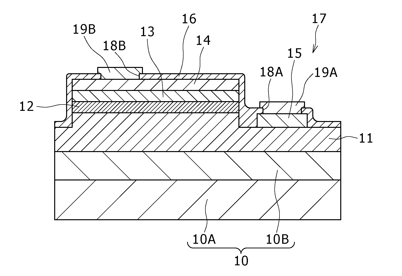
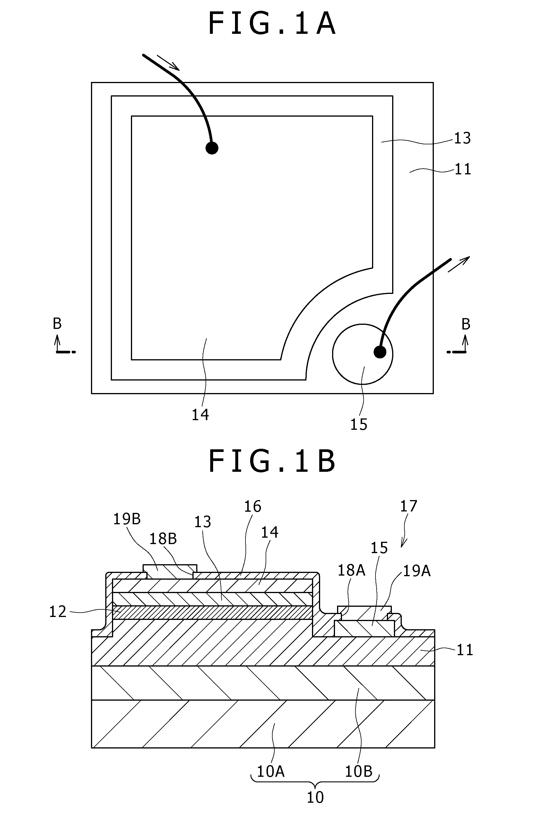
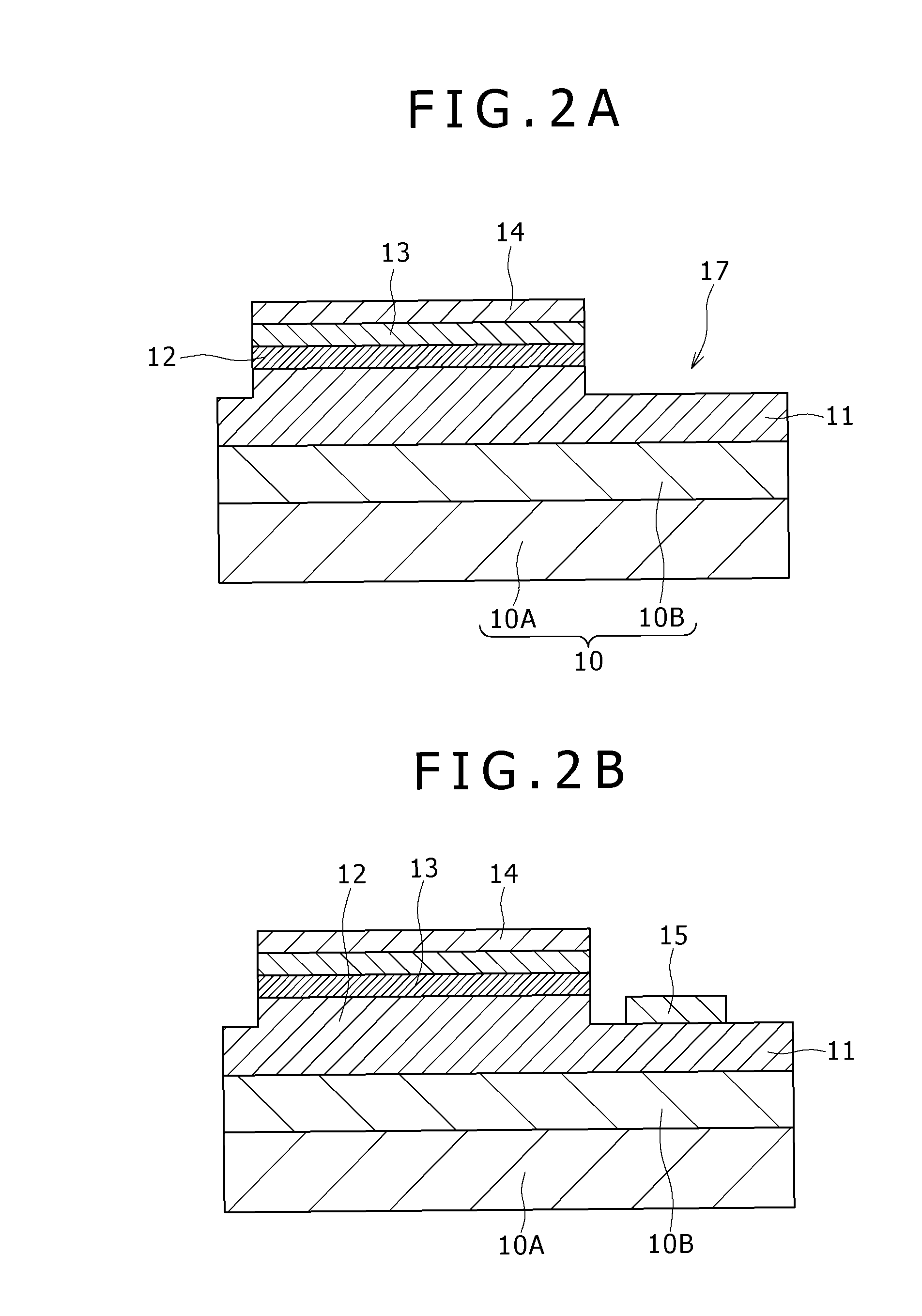
[0077]The light emitting device according to Example 1 includes a light emitting diode including GaN based compound semiconductor layers, and, as a schematic layout view of components is shown in FIG. 1A and a schematic sectional view is shown in FIG. 1B taken along line B-B of FIG. 1A, the light emitting device includes:

[0078](a) a first compound semiconductor layer 11 of a first conduction type (n type, in Example 1), an active layer 12, and a second compound semiconductor layer 13 of a second conduction type (p type, in Example 1) different from the first conduction type, which are sequentially formed over a substrate 10;

[0079](b) a first electrode 15 formed over an exposed part 17 of the first compound semiconductor layer 11; and

[0080](c) a second electrode 14 formed over the second com...

example 2

[0099]Example 2 is a modification of Example 1. In Example 2, the second electrode 14 includes a layer of silver (Ag) formed by a vacuum evaporation method and having a thickness of about 100 nm. The light emitting diode in Example 2 is of the substrate-side light pickup type, in which the light emitted from the active layer 12 is transmitted directly through the substrate 10 to go out to the exterior, or is reflected by the second electrode 14 to be transmitted through the substrate 10 and to go out to the exterior. With the second electrode 14 including silver (Ag), a reflectance of not less than 96%, for example, can be attained.

[0100]Incidentally, the other steps and the configurations and structures of the light emitting diode in Example 2 can be made to be the same as in Example 1, and detailed description of them is therefore omitted.

example 3

[0101]Example 3 is a modification of Example 1 or Example 2. In Example 3, a step of exposing the surface of the SOG layer 16 to a plasma atmosphere is further provided between [Step 140] and [Step 150]. With the surface of the SOG layer 16 thus exposed to the plasma atmosphere, organic matters (e.g., hydrocarbons) contained in the surface portion of the SOG layer 16 are removed, whereby an SOG layer 16 with high quality can be obtained. Examples of the conditions of the plasma atmosphere include the conditions shown in the following Table 1. Incidentally, the treatment of exposing the surface of the SOG layer 16 to a plasma atmosphere can similarly be carried out also in the following Examples.

[0102]

TABLE 1Plasma atmosphere:O2 gas, Ar gas, N2 gas or the like,used either singly or in combinationPressure:0.1 to 100PaApplied power:350WTreating time:10min


PUM


Abstract

Herein disclosed a method of manufacturing a light emitting device, including the steps of: (A) sequentially forming a first compound semiconductor layer of a first conduction type, an active layer, and a second compound semiconductor layer of a second conduction type different from said first conduction type, over a substrate; and (B) exposing a part of said first compound semiconductor layer, forming a first electrode over said exposed part of said first compound semiconductor layer and forming a second electrode over said second compound semiconductor layer, wherein said method further includes, subsequent to said step (B), the step of: (C) covering at least said exposed part of said first compound semiconductor layer, an exposed part of said active layer, an exposed part of said second compound semiconductor layer, and a part of said second electrode with an SOG layer.

Description

CROSS REFERENCES TO RELATED APPLICATIONS[0001]The present invention contains subject matter related to Japanese Patent Application JP 2006-284051 filed in the Japan Patent Office on Oct. 18, 2006, the entire contents of which being incorporated herein by reference.BACKGROUND OF THE INVENTION[0002]1. Field of the Invention[0003]The present invention relates to a light emitting device and a method of manufacturing the same.[0004]2. Description of the Related Art[0005]A light emitting diode (LED) according to the related art, for example, one disclosed in Japanese Utility Model No. 3068914 has a light emitting layer having a stack structure in which, for example, an under layer 10B formed based on an MOCVD method, a first compound semiconductor layer 11 of a first conduction type (e.g., n-type), an active layer 12, and a second compound semiconductor layer 13 of a second conduction type (e.g., p-type) are stacked over a substrate 10A including, for example, sapphire, as shown in a sche...

Claims


Application Information

Patent Timeline
Patent Type & Authority Patents(United States)
IPC IPC(8): H01L21/00H01L33/06H01L33/32H01L33/42
CPCH01L33/44H01L33/38
Inventor WATANABE, YOSHIAKIHINO, TOMONORIOKANO, NOBUKATAKURAMOCHI, HISAYOSHIKIKUCHI, YUICHIROOHASHI, TATSUO
Owner SONY CORP
Why Eureka
Try Eureka