In situ monitoring of wafer charge distribution in plasma processing

a plasma processing and charge distribution technology, applied in the manufacture of semiconductor/solid-state devices, basic electric elements, electric apparatus, etc., can solve the problems of difficult to remove the wafer from the chuck, unsatisfactory electric field and clamping force, and field emission tunneling across the interface gap

Inactive Publication Date: 2011-01-04
GLOBALFOUNDRIES U S INC
View PDF9 Cites 16 Cited by
  • Summary
  • Abstract
  • Description
  • Claims
  • Application Information

AI Technical Summary

Problems solved by technology

The phenomenon occurs when residual charge is left on the chuck dielectric or the wafer surface leading to undesired electric field and clamping force.
This may arise because of uncompensated direct current (DC) bias and / or charge accumulated on the chuck surface or on the wafer due to excessive local field, which may cause field emission tunneling across the interface gap.
However, if charge does not go to zero or remains above a threshold value, the resulting residual charge may make it difficult to remove the wafer from the chuck.
This sticking or de-chuck fault can create problems.
One problem created by the sticking is that the attempted lifting of the wafer off of the chuck can create “spray”.
That is, sticking can cause the wafer to be subjected to stress during the de-chucking which can damage the wafer and result in “spray”.
This can cause electrical opens due to block metal deposition.
This “spray” is undesirable and is a symptom of sticking.
However, this does not always occur and occasionally the wafer remains stuck to the ESC due to the presence of trapped charge within the ESC.
If the wafer is mechanically removed from the chamber while the ESC is in a partially clamped state, this can place stress on the wafer which causes mechanical damage and generates foreign material, commonly known as “ESC spray defects”.
These and other plasma perturbations can lead to temporal distortions in the plasma flux, causing surface charge rearrangement as measurable in the ESC bias and ESC current.
For example, the electrostatic (arc) discharges are particularly problematic within RIE, CVD, and PVD processes that result in temporal disturbances to the ion flux reaching the wafer surface.
Similarly, an arc discharge to the wafer can damage the wafer and can create a perturbation in the wafer surface charge distribution, resulting in current flow into or out of the ESC.
Such spikes in the ESC bias and ESC current are undesirable and are a symptom or indicator of a possible SPC violation.
That is, they can be indicative of a problem with the processing tool specifically a charge buildup within the tool and subsequent high voltage discharge at or near the wafer.
This results in physical damage to the internal components of the reactor, physical damage to the wafer and electrical damage to the semiconductor devices present on or within the wafer.
Although conventional RIE, CVD and PVD processing tools currently provide information about the ESC bias voltage and current, this information is not utilized to determine whether the power subsystems, ESC and other internal reactor components, (and by extension the processing tool) is functioning properly, and / or is not utilized to determine whether wafers produced by a processing tool could possibly be in violation of SPC.

Method used


Image

  • In situ monitoring of wafer charge distribution in plasma processing
  • In situ monitoring of wafer charge distribution in plasma processing
  • In situ monitoring of wafer charge distribution in plasma processing

Examples


Embodiment Construction

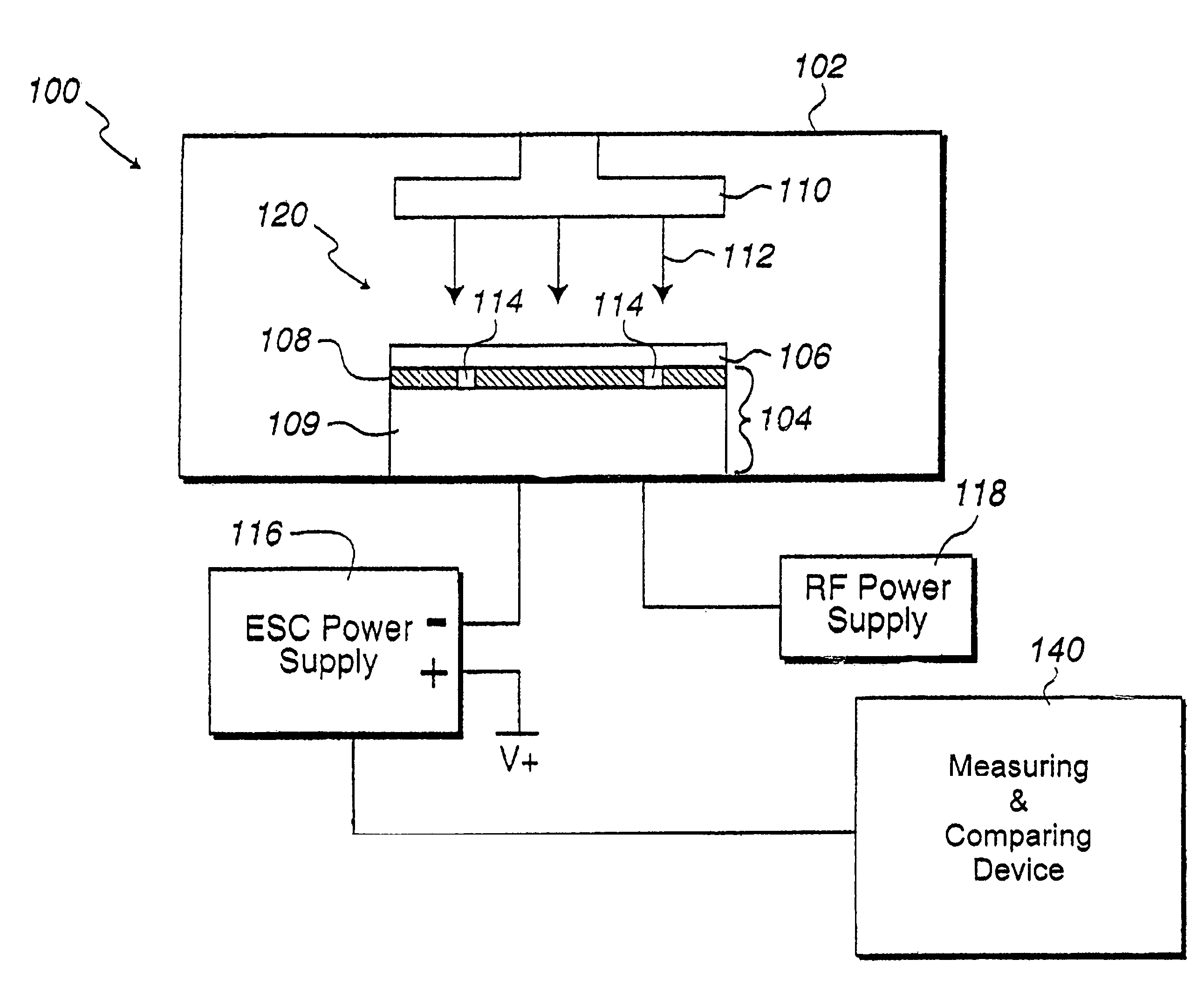
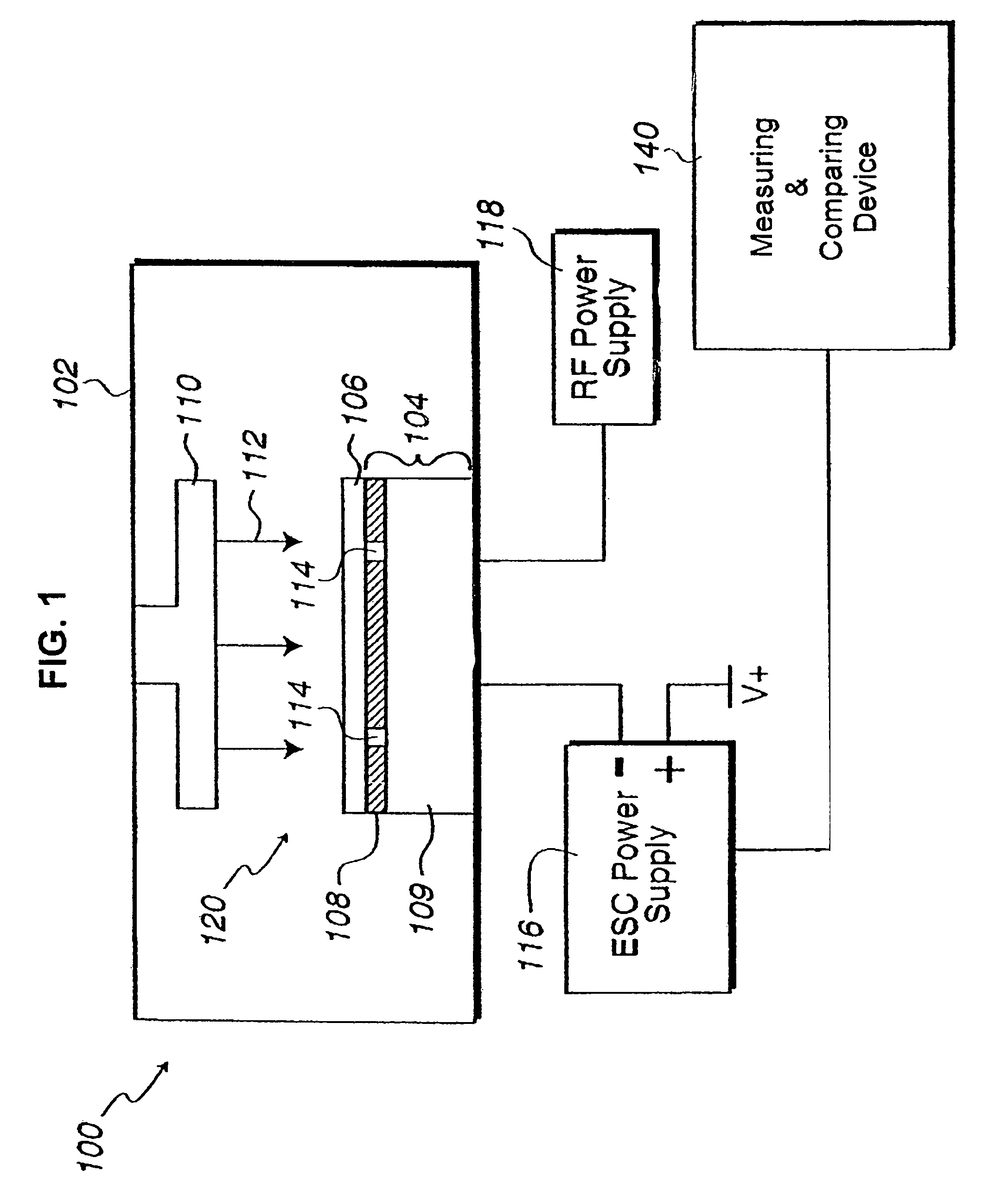
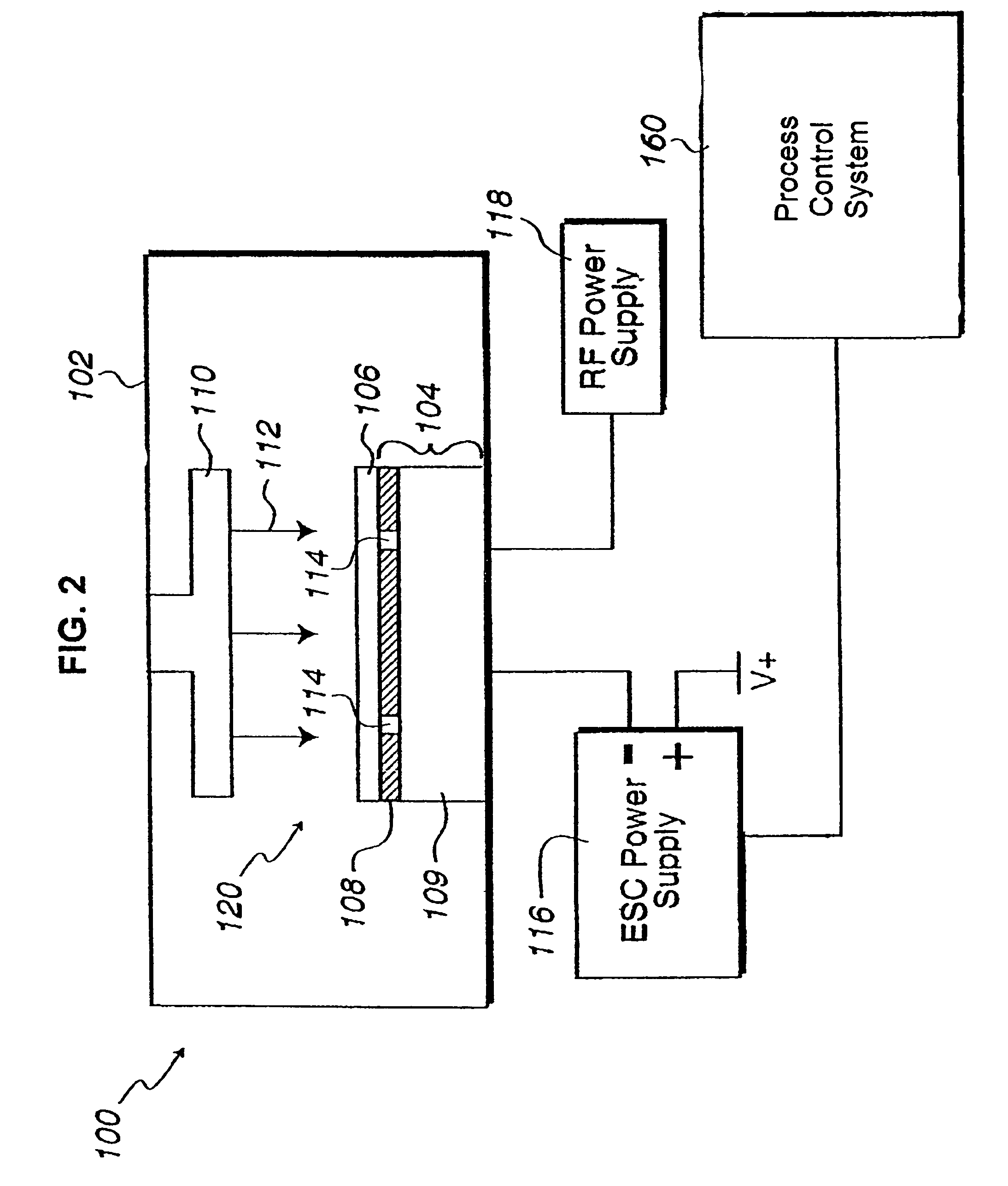
[0032]The present invention relates to the manufacture of semiconductor devices. More specifically, the present invention relates to methods and apparatuses for electrostatically clamping and declamping a semiconductor wafer on an electrostatic chuck (ESC) in a processing chamber of a semiconductor wafer processing system. The invention also aims to solve one or more of the problems noted herein by real time monitoring and multivariate processing of electrical signals from the ESC, RF and DC power subsystems present on semiconductor processing tools.

[0033]The present invention also relates to monitoring and / or detecting ESC voltage, ESC current, and / or ESC bias (e.g., by using tool trace data) in order to determine whether there is a problem with the processing tool and, in particular, whether there is a problem with the ESC (e.g., a ESC chuck default) and / or the shower head. Trace data analysis of several ESC spray events performed by Applicant indicates that the phenomenon can be ...


PUM


Abstract

A processing system and method. The processing system includes a processing tool, an electrostatic chuck (ESC) arranged within the processing tool, and a system that at least one of detects at least one of an ESC bias spike and an ESC current spike of the ESC and determines when an ESC bias voltage is zero or exceeds a threshold value. The method includes at least one of detecting at least one of an ESC bias spike and an ESC current spike of the ESC, and determining when an ESC bias voltage is zero or exceeds a threshold value. The system and method can be used in real time ESC and plasma processing diagnostics to minimize yield loss and wafer scrap.

Description

FIELD OF THE INVENTION[0001]The present invention relates to the manufacture of semiconductor devices. More specifically, the present invention relates to methods and apparatuses for electrostatically clamping and declamping a semiconductor wafer on an electrostatic chuck (ESC) in a processing chamber of a semiconductor wafer processing system. The invention also relates to monitoring and / or detecting ESC voltage, ESC current, and / or ESC bias in order to determine whether a statistical process control (SPC) violation has occurred.BACKGROUND OF THE INVENTION[0002]The use of electrostatic chucks in wafer processing systems is known. In wafer processing, wafers can be processed in a plasma processing system which may be used for etching (e.g., reactive ion etching RIE), oxidation, annodization, chemical vapor deposition (CVD), physical vapor deposition (PVD), and other processes associated with the manufacture of semiconductor wafers.[0003]The plasma processing system typically include...

Claims


Application Information

Patent Timeline
Patent Type & Authority Patents(United States)
IPC IPC(8): H01T23/00H01L21/683
CPCH01L21/67069H01L21/67253H01L21/683Y02P80/30
Inventor BOYD, KEVIN MGALLO, JAMES AHIGGINS, EDWARD PREATH, MARK LSHIFFLER, BARBARA LWONG, JUSTIN
Owner GLOBALFOUNDRIES U S INC
Why Eureka
Try Eureka