Semiconductor storage device

a technology of semiconductor devices and storage devices, applied in semiconductor devices, digital storage, instruments, etc., can solve the problems of information destruction and essentially slow rewriting speed of such devices

Inactive Publication Date: 2011-01-04
RENESAS ELECTRONICS CORP
View PDF9 Cites 169 Cited by
  • Summary
  • Abstract
  • Description
  • Claims
  • Application Information

AI Technical Summary

Benefits of technology

[0024]Effects of typical ones of the inventions disclosed in the present application will be briefly described as follows.
[0025](1) A high-speed readable and high-capacity non-volatile semiconductor storage device can be realized by using a semiconductor integrated circuit device utilizing a technique of the present invention.
[0026](2) Also, a high-reliability and high-performance micro-processor for embedded applications can be provided by mixedly mounting the device on the same substrate that a semiconductor logic computing device is provided on.
[0027](3) Further, the device can be provided as a single chip.BRIEF DESCRIPTIONS OF THE DRAWINGS
[0028]FIGS. 1A to 1E are diagrams showing structures, a circuit frame diagram, and operation methods of a storage device in a semiconductor storage device according to a first embodiment of the present invention;
[0029]FIGS. 2A and 2B are diagrams showing a structure and a circuit of a conventional method, respectively;

Problems solved by technology

However, since a rewriting speed thereof is essentially slow, it is mainly used as a programmable ROM, an information storage device for a still camera, in which the rewriting is not frequently performed, or the like.
Also, since the FLASH memory requires large power consumption at the rewriting time, it includes a large issue from the viewpoint of reduction of battery exhaustion which is important for mobile terminal equipment.
However, when the chalcogenide is in the reset state, the information is destroyed.

Method used


Image

  • Semiconductor storage device
  • Semiconductor storage device
  • Semiconductor storage device

Examples


first embodiment

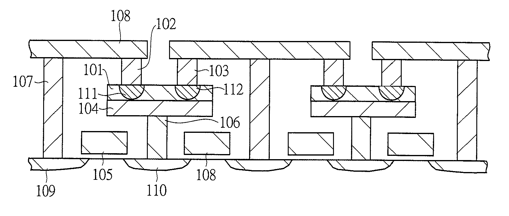
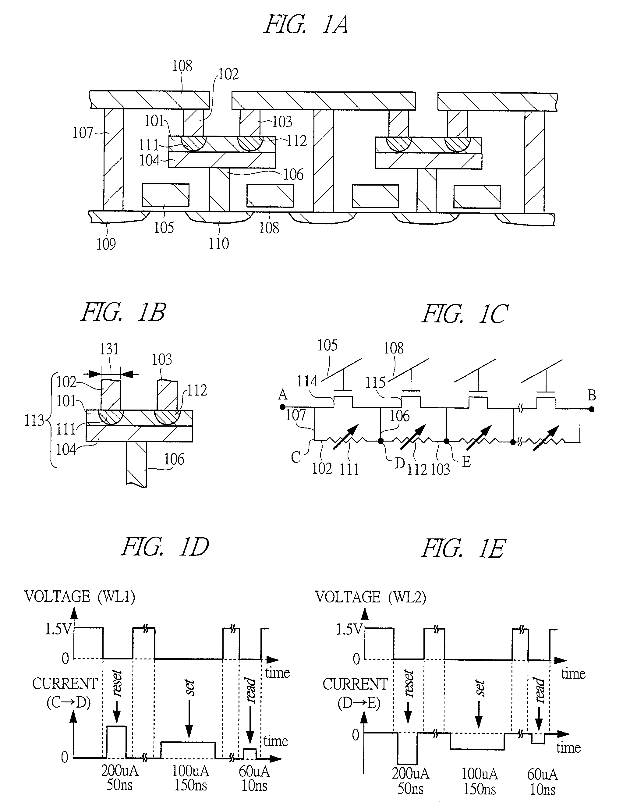
[0061]Each of FIGS. 1A, 1B, and 1C shows a structure of a storage device array used in a semiconductor storage device of the present invention. A phase change thin film (chalcogenide) 101 is sandwiched between an upper plug electrode 102 and a lower electrode 104. A composition of the phase change thin film 101 is Ge2Sb2Te5, and compositions of the upper plug electrode 102 and the lower electrode 104 are tungsten. A plug size 131 is a diameter of 160 nm. The plug size varies according to a generation of a semiconductor process to be used. Although tungsten is frequently used as the composition of the upper plug electrode 102, any material can be used as long as having conductivity.

[0062]Each of FIGS. 1D and 1E shows a procedure when a writing and a reading is performed to a memory cell configuring the circuit shown in FIG. 1C. First, all word line voltages are set to 1.5 V to set all selecting transistors to be ON state. Next, a pulse of 0 V is applied to a word line 105 (WL1) of a ...

second embodiment

[0097]Regarding a memory cell having a structure not required for switching the direction of the current carry when the adjacent cell is selected to perform the writing operation in spite of having a configuration of the same equivalent circuit as that of the first embodiment, a description thereof will be described below.

[0098]FIG. 10 shows a layout of a principal part of a memory cell according to a second embodiment. Such a structure is manufactured that a plug 1005 contacted to a chalcogenide 1004 and a plug 1002 contacted to a diffusion layer of a transistor have a word line 1003 therebetween and are connected by a wiring layer 1006 inside an active region 1001 to form one memory cell. If it is assumed that a minimum feature size is “F”, a distance between adjacent word lines is 2F.

[0099]The above-described memory cell is connected in series to a memory cell including a wiring layer 1007 adjacent thereto manufactured inside the same active region 1001 via the diffusion layer, s...

third embodiment

[0108]FIG. 17 shows a schematic diagram of a configuration of a phase change memory according to a third embodiment. That is, the phase change memory is configured with a memory array, a multiplexer MUX, a row decoder XDEC, a column decoder YDEC, a reading circuit RC, and a rewriting circuit PRGM0. The memory array is configured with memory blocks MB00 to MBmn configured with a plurality of memory cells. In the same figure, memory blocks configured with eight memory cells MC0 to MC7 is shown as one example. Each of the memory cells is arranged at each intersection of bit lines BL0 to BLn and word lines WL00 to WL07, . . . , WLm0 to WLm7 to be destinations of output signals from the row decoder XDEC0 and between the bit lines BL0 to BLn and source lines (here, SL12 and SL34). Each of the source lines is shared by memory blocks adjacent to each other. The memory block further includes a hierarchy switch HS0 inserted between a bit line and a memory cell. The hierarchy switch HS0 is con...


PUM


Abstract

In a semiconductor storage device such as a phase change memory, a technique which can realize high integration is provided. The semiconductor storage device includes a phase change thin film 101 having two stable phases of a crystal state with low electric resistance and an amorphous state with high electric resistance, upper plug electrodes 102 and 103 provided on one side of the phase change thin film 101, a lower electrode 104 provided on the other side of the phase change thin film 101, a selecting transistor 114 whose drain / source terminals are connected to the upper plug electrode 102 and the lower electrode 104, and a selecting transistor 115 whose drain / source terminals are connected to the upper plug electrode 103 and the lower electrode 104, and a first memory cell is configured with the selecting transistor 114 and a phase change region 111 in the phase change thin film 101 sandwiched between the upper plug electrode 102 and the lower electrode 104, and a second memory cell is configured with the selecting transistor 115 and a phase change region 112 in the phase change thin film 101 sandwiched between the upper plug electrode 103 and the lower electrode 104.

Description

TECHNICAL FIELD[0001]The present invention relates to a semiconductor storage device, and more particularly, the present invention relates to a technique effectively applied to a semiconductor integrated circuit device having: a high density integrated memory circuit including a memory cell using a phase change material particularly represented by a chalcogenide material; a logic mixedly mounted memory in which a memory circuit and a logic circuit are provided on the same semiconductor substrate; or an analog circuit. Particularly, the present invention relates to a structure in which memory cells are arranged in high density so that a high-speed drive can be achieved.BACKGROUND ART[0002]A semiconductor nonvolatile memory is frequently used for mobile equipment such as a mobile phone, and in recent years, a market thereof has been increasingly spread. Currently, the semiconductor nonvolatile memory which is most utilized is a FLASH memory. However, since a rewriting speed thereof is...

Claims


Application Information

Patent Timeline
Patent Type & Authority Patents(United States)
IPC IPC(8): G11C11/00
CPCG11C13/0004G11C13/0069H01L27/2436H01L27/2463H01L27/2472H01L45/06H01L45/1233H01L45/144G11C2213/75H10B63/30H10B63/80H10B63/82H10N70/231H10N70/826H10N70/8828
Inventor FUJISAKI, YOSHIHISAHANZAWA, SATORUKUROTSUCHI, KENZOMATSUZAKI, NOZOMUTAKAURA, NORIKATSU
Owner RENESAS ELECTRONICS CORP
Why Eureka
Try Eureka