Micro free electron laser (FEL)

a free electron laser and micro-electrode technology, applied in the direction of accelerators, laser details, electric discharge tubes, etc., can solve the disadvantage of high-speed electrons

Inactive Publication Date: 2011-01-25
ADVANCED PLASMONICS
View PDF361 Cites 10 Cited by
  • Summary
  • Abstract
  • Description
  • Claims
  • Application Information

AI Technical Summary

Problems solved by technology

However, the need for high velocity electrons is disadvantageous.

Method used


Image

  • Micro free electron laser (FEL)
  • Micro free electron laser (FEL)
  • Micro free electron laser (FEL)

Examples


first embodiment

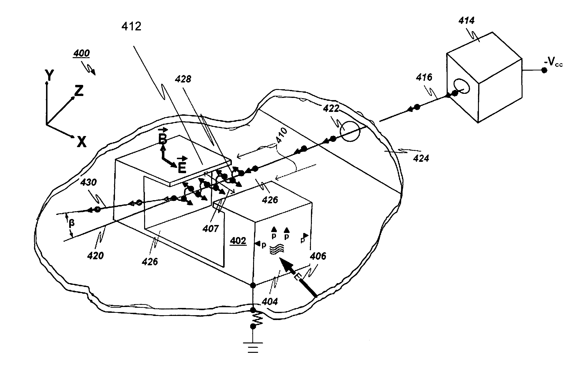
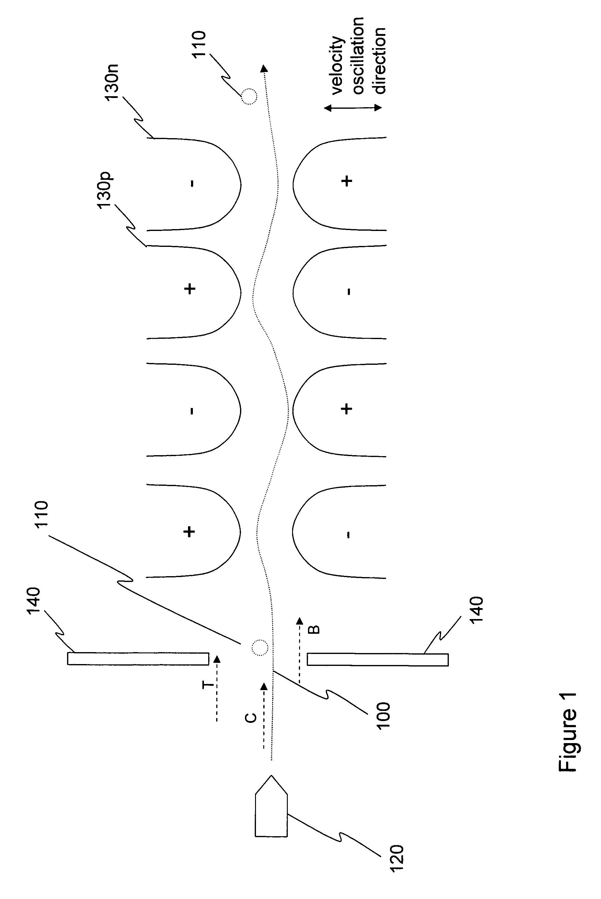
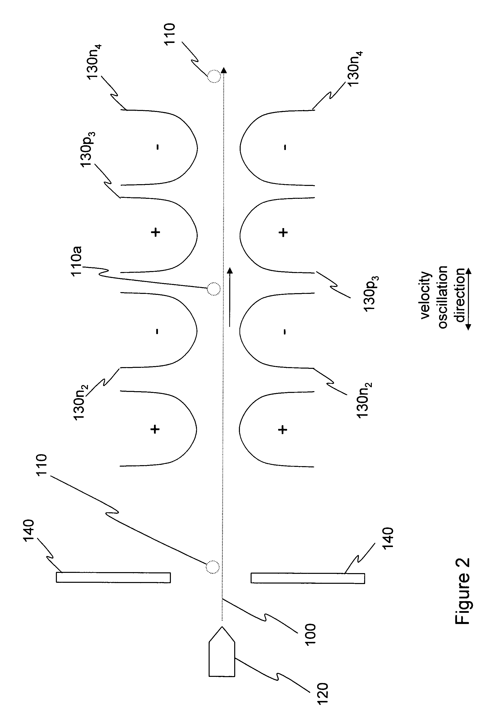
[0020]Turning now to the drawings, FIG. 1 is a high-level conceptual representation of a charged particle moving through a series of alternating electric fields according to the present invention. As shown therein, a charged particle beam 100 including charged particles 110 (e.g., electrons) is generated from a charged particle source 120. (The charged particle beam 100 can include ions (positive or negative), electrons, protons and the like. The beam may be produced by any source, including, e.g., without limitation an ion gun, a thermionic filament, a tungsten filament, a cathode, a planar vacuum triode, an electron-impact ionizer, a laser ionizer, a chemical ionizer, a thermal ionizer, an ion-impact ionizer)

[0021]As the beam 100 is projected, it passes between plural alternating electric fields 130p and 130n. The fields 130p represent positive electric fields on the upper portion of the figure, and the fields 130n represent negative electric fields on the upper portion of the fig...

second embodiment

[0036]In light of the variation in paths that a charged particle can undergo based on its initial path between electrodes 140, in a coherent radiation source, a focusing element 700 is added in close proximity to the electrodes 140. The focusing element 700, while illustrated before the electrodes 140 may instead be placed after. In such a configuration, additional charged particles may traverse a center path between the fields and undergo constructive interference.

third embodiment

[0037]In a coherent light source, a pre-bunching element 800 is added which helps to control the inter-arrival time between charged particles, and therefore aid in the production of coherent Electromagnetic Radiation (EMR). One possible configuration of a pre-bunching element 800 is a resonant structure such as is described in U.S. application Ser. No. 11 / 410,924, entitled “Selectable Frequency EMR Emitter,” filed on even date herewith and incorporated herein by reference. However, exemplary resonant structures are shown in FIGS. 9A-9H. As shown in FIG. 9A, a resonant structure 910 may comprise a series of fingers 915 which are separated by a spacing 920 measured as the beginning of one finger 915 to the beginning of an adjacent finger 915. The finger 915 has a thickness that takes up a portion of the spacing between fingers 915. The fingers also have a length 925 and a height (not shown). As illustrated, the fingers of FIG. 9A are perpendicular to the beam 100.

[0038]Resonant struct...


PUM


Abstract

A charged particle beam including charged particles (e.g., electrons) is generated from a charged particle source (e.g., a cathode or scanning electron beam). As the beam is projected, it passes between plural alternating electric fields. The attraction of the charged particles to their oppositely charged fields accelerates the charged particles, thereby increasing their velocities in the corresponding (positive or negative) direction. The charged particles therefore follow an oscillating trajectory. When the electric fields are selected to produce oscillating trajectories having the same (or nearly the same) frequency as the emitted radiation, the resulting photons can be made to constructively interfere with each other to produce a coherent radiation source.

Description

CROSS-REFERENCE TO CO-PENDING APPLICATIONS[0001]The present invention is related to the following co-pending U.S. Patent applications: (1) U.S. patent application Ser. No. 11 / 238,991, entitled “Ultra-Small Resonating Charged Particle Beam Modulator,” and filed Sep. 30, 2005; (2) U.S. patent application Ser. No. 10 / 917,511, filed on Aug. 13, 2004, entitled “Patterning Thin Metal Film by Dry Reactive Ion Etching,”; (3) U.S. application Ser. No. 11 / 203,407, filed on Aug. 15, 2005, entitled “Method Of Patterning Ultra-Small Structures”; (4) U.S. application Ser. No. 11 / 243,476, entitled “Structures And Methods For Coupling Energy From An Electromagnetic Wave,” filed on Oct. 5, 2005; (5) U.S. application Ser. No. 11 / 243,477, entitled “Electron Beam Induced Resonance,” filed on Oct. 5, 2005, and (6) U.S. application Ser. No. 11 / 411,130, entitled “Charged Particle Acceleration Apparatus and Method,” filed on even date herewith, all of which are commonly owned with the present application a...

Claims


Application Information

Patent Timeline
Patent Type & Authority Patents(United States)
IPC IPC(8): H01S3/00
CPCH01J25/00H01S3/0903H05H7/04H05H15/00
Inventor GORRELL, JONATHANDAVIDSON, MARKMAINES, MICHAEL E.
Owner ADVANCED PLASMONICS
Why Eureka
Try Eureka