Systems, methods, and apparatuses for complementary metal oxide semiconductor (CMOS) antenna switches using body switching in multistacking structure

a technology of metal oxide semiconductor and antenna switch, which is applied in the field of complementary metal oxide semiconductor (cmos) antenna switch, can solve the problems of radio frequency switch, current cmos technology presents a variety of difficulties, and cmos technology from being used for rf switch, and achieves low insertion loss, high power handling capability, and high blocking capability.

Inactive Publication Date: 2011-02-15
SAMSUNG ELECTRO MECHANICS CO LTD +1
View PDF27 Cites 41 Cited by
  • Summary
  • Abstract
  • Description
  • Claims
  • Application Information

AI Technical Summary

Benefits of technology

[0006]Embodiments of the invention may provide for CMOS RF switches, which may be referred to as a CMOS SP4T switch. According to an embodiment of the invention, the CMOS RF switch may be fabricated using a 0.18 um process, although other processes may be utilized without departing from the invention. In order to provide high power handling capability in a multi-band operation (e.g., about 900 MHz and 1.9 GHz) of the CMOS RF switch, an multi-stacked transistors with substrate body switching may be applied to the receiver switch. According to an embodiment of the invention, the CMOS RF switch may provide higher blocking capability at the transmission (Tx) mode as well as low insertion loss at the reception (Rx) mode at multi-band (e.g., 900 MHz and 1.9 GHz).

Problems solved by technology

Two significant mobile application components—power amplifiers (PAs) and radio frequency (RF) switches—have not yet been commercially integrated into CMOS technology.
However, current CMOS technology presents a variety of difficulties for its application to RF switches.
In particular, CMOS material characteristics, including lossy substrates due to low mobility of electrons and low breakdown voltages due to p-n junction, hot carrier effects, have prevented CMOS technology from being used for RF switches that require multi-band operation, high power levels, and / or integration with other devices and circuits.

Method used


Image

  • Systems, methods, and apparatuses for complementary metal oxide semiconductor (CMOS) antenna switches using body switching in multistacking structure
  • Systems, methods, and apparatuses for complementary metal oxide semiconductor (CMOS) antenna switches using body switching in multistacking structure
  • Systems, methods, and apparatuses for complementary metal oxide semiconductor (CMOS) antenna switches using body switching in multistacking structure

Examples


Embodiment Construction

[0020]The invention now will be described more fully hereinafter with reference to the accompanying drawings, in which some, but not all embodiments of the invention are shown. Indeed, these inventions may be embodied in many different forms and should not be construed as limited to the embodiments set forth herein; rather, these embodiments are provided so that this disclosure will satisfy applicable legal requirements. Like numbers refer to like elements throughout.

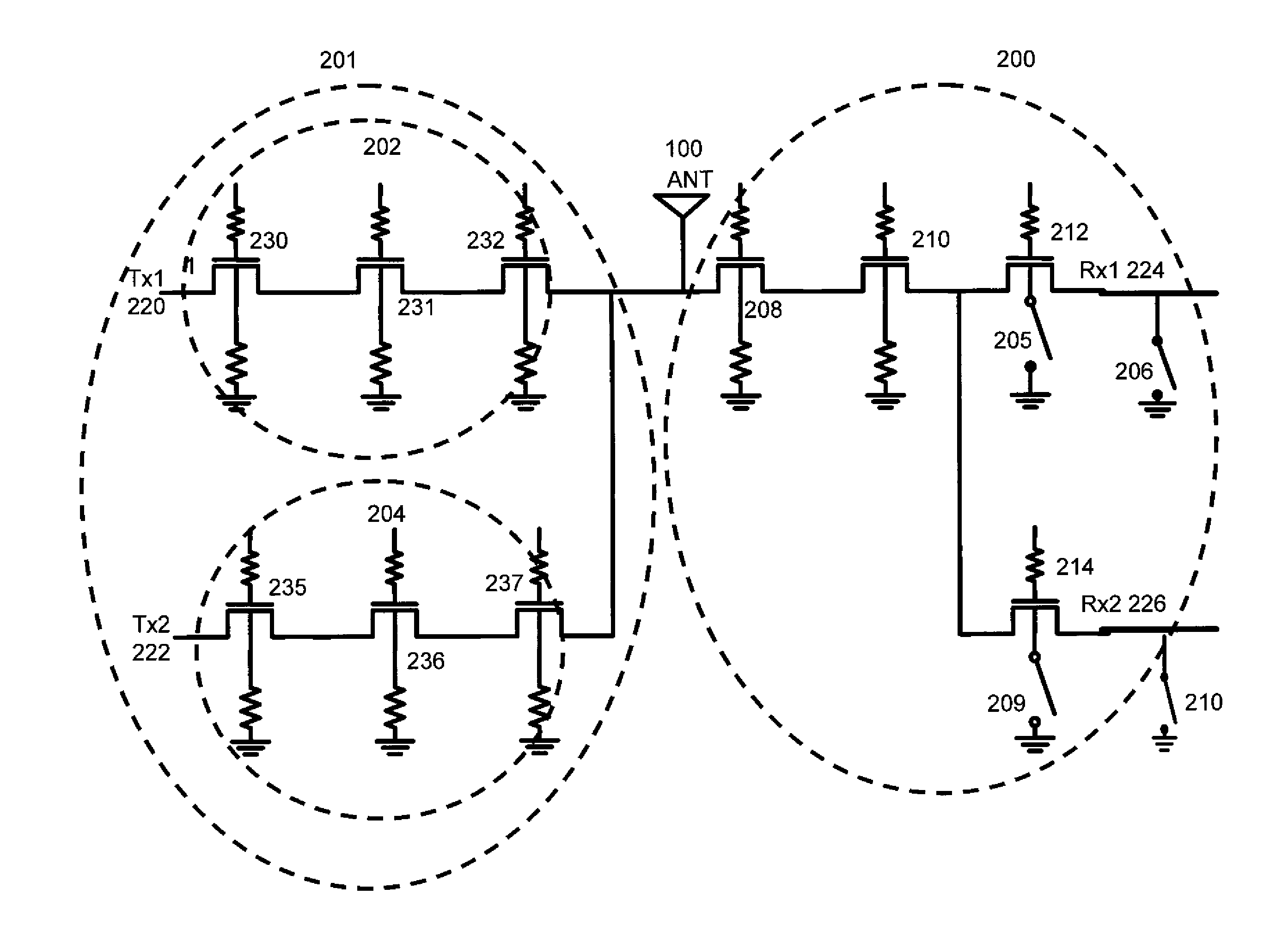
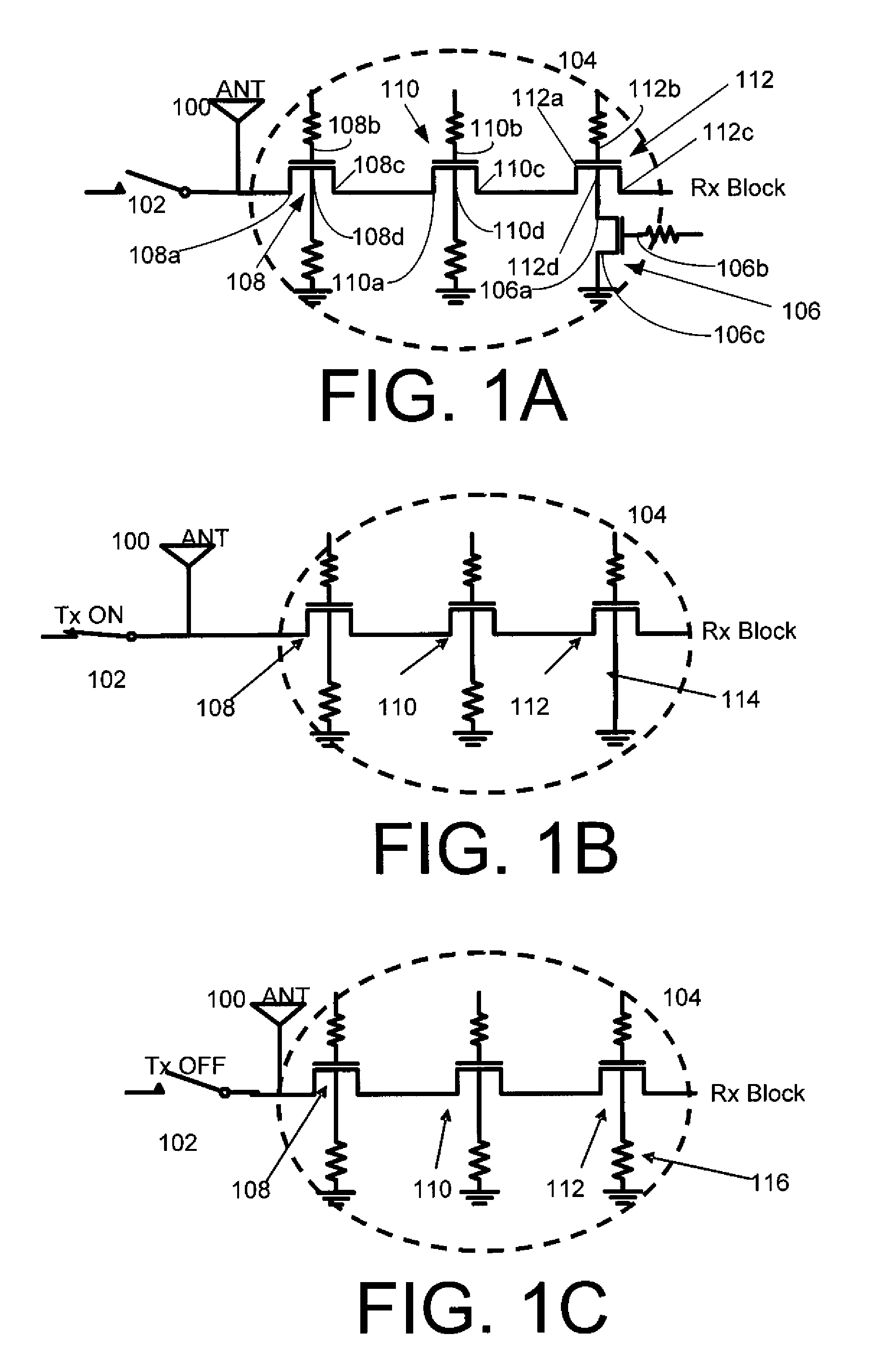
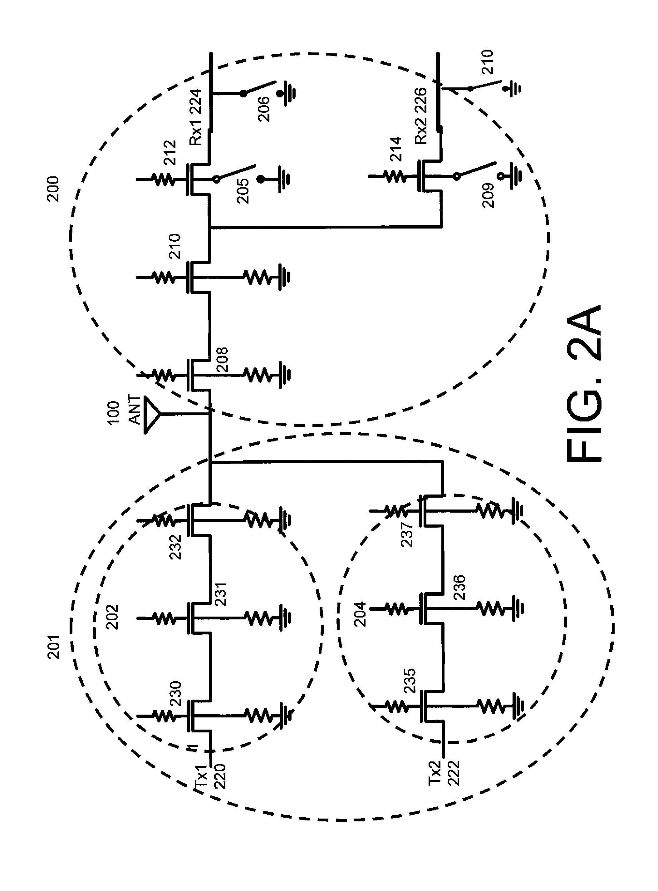
[0021]Embodiments of the invention may provide for CMOS RF antenna switches, which may also be referred to as SP4T CMOS switches. The CMOS RF antenna switches in accordance with embodiments of the invention may provide for one or more of multi-band operation, high power level handling, and integration with other devices and circuits. Generally, the CMOS RF antenna switch may include a receiver switch and a transmit switch. The receiver switch may utilize one or more switching substrate bodies, as will be described in fu...


PUM


Abstract

Embodiments of the invention may provide for a CMOS antenna switch, which may be referred to as a CMOS SP4T switch. The CMOS antenna switch may operate at a plurality of frequencies, perhaps around 900 MHz and 1.9 GHz according to an embodiment of the invention. The CMOS antenna switch may include both a receiver switch and a transmit switch. The receiver switch may utilize a multi-stack transistor with body substrate tuning to block high power signals from the transmit path as well as to maintain low insertion loss at the receiver path. On the other hand, in the transmit switch, a body substrate tuning technique may be applied to maintain high power delivery to the antenna. Example embodiments of the CMOS antenna switch may provide for 31 dBm P 1 dB at both bands (e.g., 900 MHz and 1.8 GHz). In addition, a 0.9 dB and −1.1 dB insertion loss at 900 MHz and 1.9 GHz, respectively, may be obtained according to example embodiments of the invention.

Description

RELATED APPLICATION[0001]The present application claims priority to U.S. Provisional Application Ser. No. 60 / 827,931, filed on Oct. 3, 2006, and entitled “Complementary Metal Oxide Semiconductor (CMOS) Antenna Switches using Body Switching in Multistacking Structure,” which is hereby incorporated in its entirety by reference.FIELD OF THE INVENTION[0002]The invention relates generally to antenna switches, and more particularly, to CMOS (complementary metal oxide semiconductor) antenna switches.BACKGROUND OF THE INVENTION[0003]In the past decade, the wireless communication industry has experienced explosive growth, which has in turn accelerated the development of integrated circuit (IC) industry. In particular, in the IC industry, many mobile application systems like low noise amplifiers (LNAs), mixers, and voltage-controlled oscillators (VCOs) have been integrated into CMOS technology. Two significant mobile application components—power amplifiers (PAs) and radio frequency (RF) switc...

Claims


Application Information

Patent Timeline
Patent Type & Authority Patents(United States)
IPC IPC(8): H04B1/44
CPCH03K17/063H03K17/102H03K17/693H04B1/48H03K2217/0018
Inventor AHN, MINSIKLEE, CHANG-HOCHO, CHANGHYUKCHANG, JAEJOONWOO, WANGMYONGKIM, HAKSUNLASKAR, JOY
Owner SAMSUNG ELECTRO MECHANICS CO LTD
Why Eureka
Try Eureka