Method to produce an electrical model of an integrated circuit substrate and related system and article of manufacture

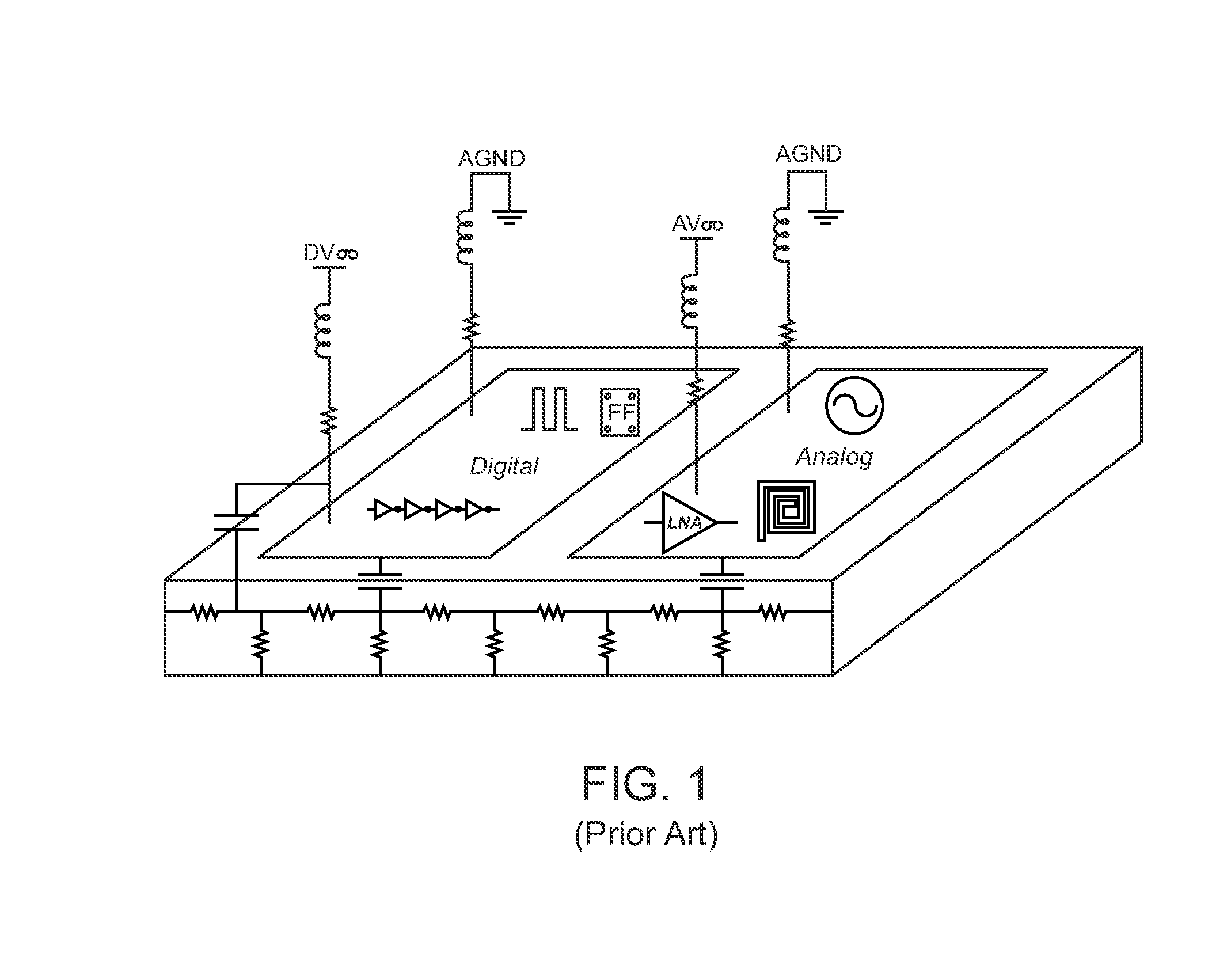
a technology of integrated circuits and electrical models, applied in the direction of electric/magnetic computing, analogue processes for specific applications, instruments, etc., can solve the problems of unintended interaction between digital and analog, lack of degree, and degradation of analog performan

Inactive Publication Date: 2011-03-01
CADENCE DESIGN SYST INC
View PDF8 Cites 16 Cited by
  • Summary
  • Abstract
  • Description
  • Claims
  • Application Information

AI Technical Summary

Benefits of technology

[0021]These and other features and advantage of the invention will become more apparent from the following detailed description thereof in conjunction with the appended drawings.

Problems solved by technology

Substrate noise can result in un-intended interaction between the digital and analog components of a chip through the underlying silicon substrate.
Analog systems generally lack the degree of noise immunity of digital circuits, and the substrate coupling noise can degrade analog performance.
Substrate noise can cause fluctuations in the voltage potential of the substrate, which can affect CMOS device behavior.
For a digital circuit, this could result in a small change in the delay of a logic gate.
However, for an analog circuit, the effect can be much more severe.
For instance, in an amplifier, a change in threshold voltage can change the operating point of the amplifier and significantly reduce the gain.
Digital circuit switching generates substrate noise through multiple mechanisms.
For instance, digital circuit switching results in substrate noise injection to the substrate from the junction of a digitally switching transistor.
Also, digital circuit switching results in substrate noise injection due to power supply fluctuations.
These discharge currents work in tandem with the parasitics of the power and ground lines to cause ringing in the supplies.
However, since the substrate is connected to power and ground through low resistance substrate contacts, any such noise that appears on the power and ground lines appears also directly in the substrate.
Although noise may be attenuated by the resistance of the substrate, it still can reach all areas of the chip.
Substrate voltage fluctuations that reach analog transistors can have a detrimental impact upon their operation as described above.
Identification of substrate noise sources through simulation was especially challenging since it required not only knowledge of digital switching activity, but also identification of the actual source and physical location of the noise injectors that cause noise.
Identification of the noise sources and their locations using circuit simulation could be particularly difficult.
Since this information often is not available until later in the design flow, it often was impractical to do perform satisfactorily accurate shape based extraction earlier in the design process.
Moreover, such detailed extraction can be quite expensive in terms of run time and memory requirements.
As a result, estimates of substrate noise not only could be expensive, but also could be less effectual earlier in the design process before the availability of accurate detailed information concerning the substrate.

Method used


Image

  • Method to produce an electrical model of an integrated circuit substrate and related system and article of manufacture
  • Method to produce an electrical model of an integrated circuit substrate and related system and article of manufacture
  • Method to produce an electrical model of an integrated circuit substrate and related system and article of manufacture

Examples


Embodiment Construction

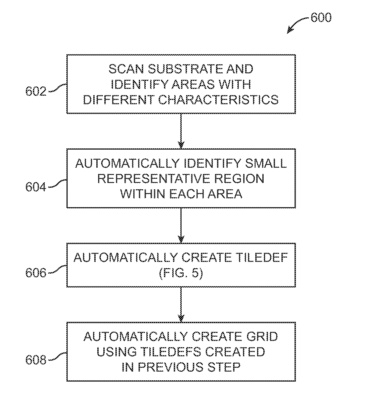
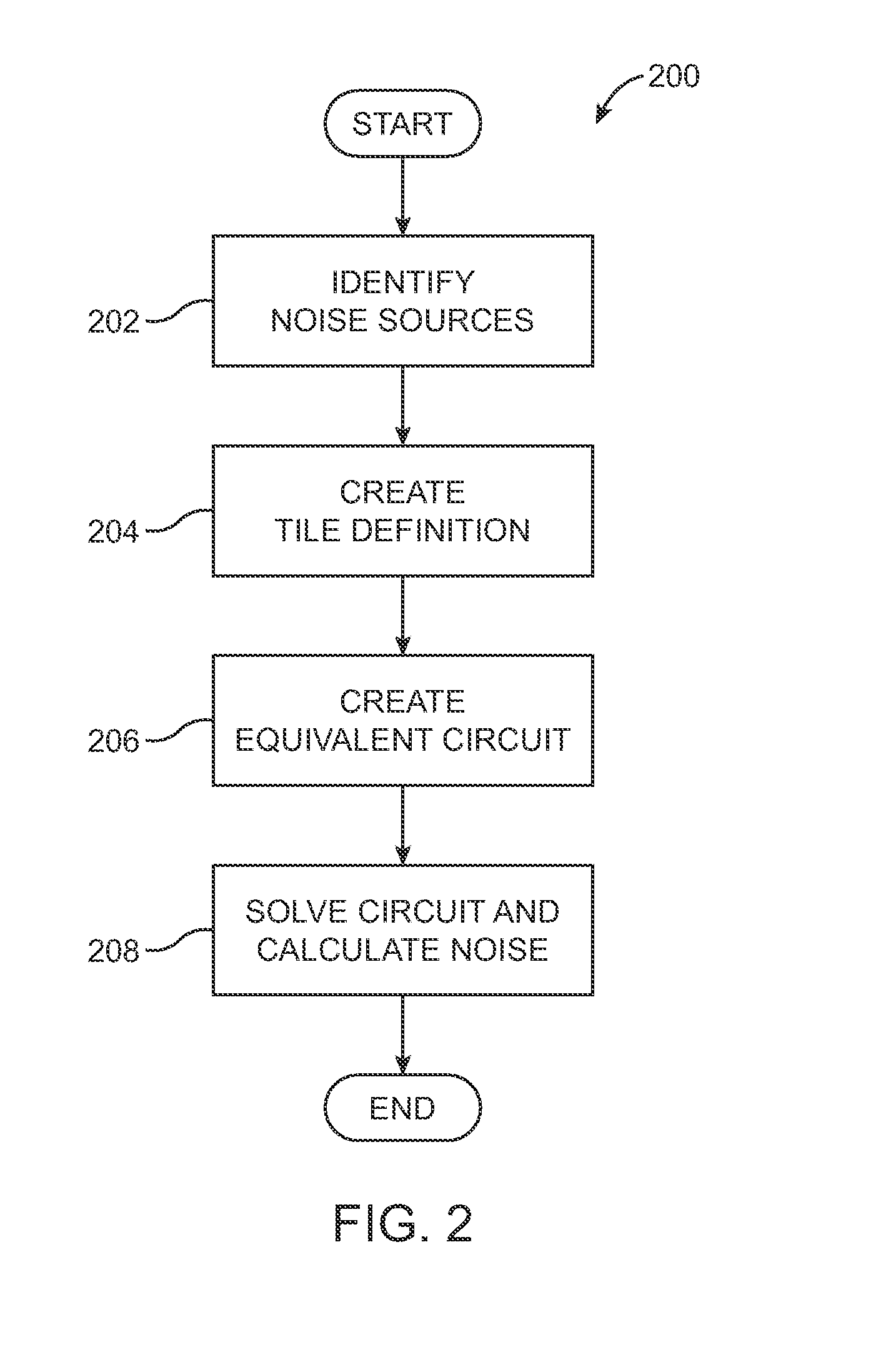
[0039]The following description is presented to enable any person skilled in the art to make and use a computer implemented method to produce a substrate noise model and a related system and article of manufacture in accordance with embodiments of the invention, and is provided in the context of particular applications and their requirements. Various modifications to the preferred embodiments will be readily apparent to those skilled in the art, and the generic principles defined herein may be applied to other embodiments and applications without departing from the spirit and scope of the invention. Moreover, in the following description, numerous details are set forth for the purpose of explanation. However, one of ordinary skill in the art will realize that the invention might be practiced without the use of these specific details. In other instances, well-known structures and processes are shown in block diagram form in order not to obscure the description of the invention with u...


PUM


Abstract

A method is provided to produce a model of an integrated circuit substrate, the method comprising: providing a tile definition that specifies an electrical model associated with instances of the tile; mapping a plurality of respective tile instances to respective locations of the substrate; and connecting the mapped tile instances to each other to produce a tile grid that models overall electrical behavior of the substrate.

Description

CROSS REFERENCE TO RELATED APPLICATION[0001]The subject matter of this application is related to that of commonly owned U.S. patent application Ser. No. 11 / 769,670, entitled METHOD AND APPARATUS FOR SUBSTRATE NOISE ANALYSIS USING SUBSTRATE TILE MODEL AND TILE GRID, filed Jun. 27, 2007, which is expressly incorporated herein by this reference.BACKGROUND OF THE INVENTION[0002]1. Field of the Invention[0003]The invention relates in general to simulation during design of integrated circuits and more particularly, to simulation to estimate integrated circuit substrate noise.[0004]2. Description of the Related Art[0005]FIG. 1 is an illustrative perspective view of a mixed-signal integrated circuit that includes a digital subsystem and an analog subsystem and that also includes a cross-section view of the IC substrate. The digital and analog subsystems are physically separated in different circuit blocks. Even though the digital and analog blocks of the integrated circuit (IC) may be separ...

Claims


Application Information

Patent Timeline
Patent Type & Authority Patents(United States)
IPC IPC(8): G06F17/50G06F9/45
CPCG06F17/5036G06F30/367
Inventor KARIAT, VINODDONG, XIAOPENGNOICE, DAVID
Owner CADENCE DESIGN SYST INC
Why Eureka
Try Eureka