Method of manufacturing semiconductor chip using laser light and plasma dicing

a laser light and plasma dicing technology, applied in the direction of semiconductor devices, basic electric elements, electrical appliances, etc., can solve the problems of limited purpose characteristics of subject to be removed, impede improvement in productivity, and increase the total number of processing steps, so as to achieve the effect of high efficiency

Active Publication Date: 2011-03-15
PANASONIC CORP
View PDF10 Cites 184 Cited by
  • Summary
  • Abstract
  • Description
  • Claims
  • Application Information

AI Technical Summary

Benefits of technology

[0009]As a consequence, the present invention has an object to provide a semiconductor chip manufacturing method capable of removing test patterns in a higher efficiency in simple steps, while a general-purpose characteristic can be secured.
[0011]In accordance with the present invention, the protection sheet which constitutes the mask in the plasma etching process is adhered onto the front plane of the semiconductor wafer, on which the integrated circuits have been formed; since the laser light is irradiated from the side of the protection sheet along the scribe lines of the semiconductor wafer on which the protection sheet has been adhered, only the predetermined widths of the protection sheet on the scribe lines are removed so as to form the mask; and also, the test patterns are removed in combination with the front plane layer of the semiconductor wafer by the above-described laser light. As a result, the test patterns can be removed in the higher efficiency in the simple steps, while the general-purpose characteristic can be secured.

Problems solved by technology

Moreover, the conventional technical ideas described in the above-explained patent publications contain the following difficult points: That is, in the conventional example disclosed in the patent publication 1, since the cutting works by employing two sorts of the rotary blades are required in the dicing step, a total number of the processing steps is increased, so that the improvement in the productivity is impeded.
As a result, there is such a difficult point as to the general-purpose characteristic that the subject to be removable is limited.
As previously explained, in the conventional semiconductor chip manufacturing methods, there is the below-mentioned problem: That is, while the general-purpose characteristic is secured, the test patterns in the dicing step can be hardly removed in a higher efficiency and in simple steps.

Method used


Image

  • Method of manufacturing semiconductor chip using laser light and plasma dicing
  • Method of manufacturing semiconductor chip using laser light and plasma dicing
  • Method of manufacturing semiconductor chip using laser light and plasma dicing

Examples


Embodiment Construction

[0021]Next, a description is made of embodiment modes of the present invention with reference to drawings.

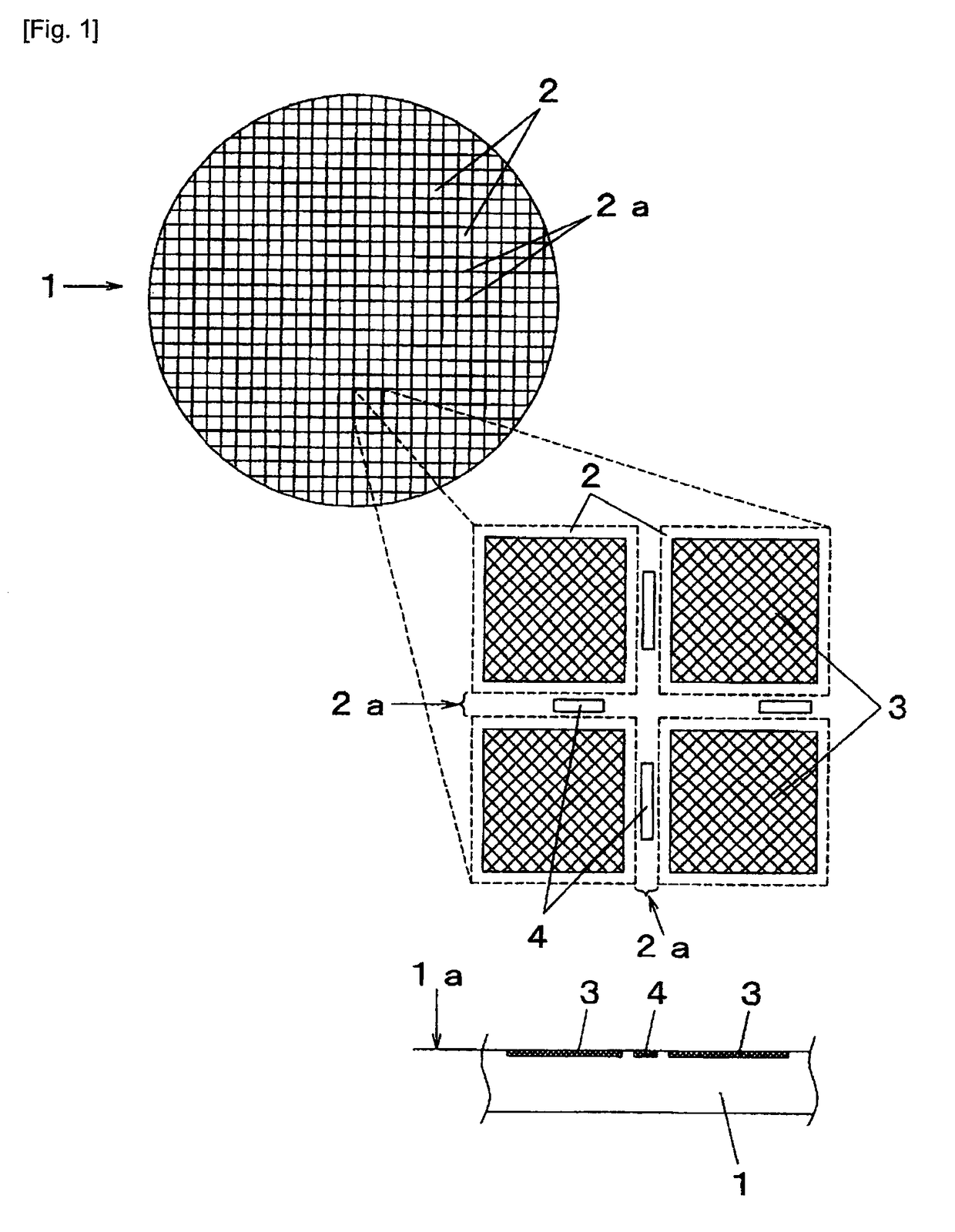
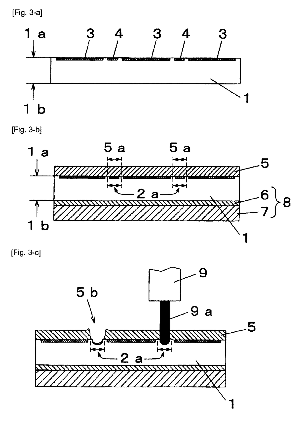
[0022]A first description is made of a semiconductor wafer 1 with reference to FIG. 1, which is employed in a semiconductor chips manufacturing method according to the present embodiment mode of the present invention. In FIG. 1, the semiconductor wafer 1 has been segmented into a plurality of chip regions 2 (areas) having rectangular shapes by employing scribe lines 2a arrayed in a lattice shape so as to cut off respective semiconductor chips from each other. On a front plane 1a corresponding to a circuit forming plane of the semiconductor wafer 1, each of integrated circuits 3 has been formed in each of the chip regions 2, and test patterns 4 have been formed in the scribe lines 2a. The test patterns 4 are employed for characteristic tests and the like in manufacturing steps of semiconductor chips, and are removed after the function of the test patterns 4 has been accomplished....


PUM


Abstract

In a method in which a semiconductor wafer 1 having integrated circuits 3 formed in a plurality of chip regions and test patterns 4 formed in scribe lines 2a is divided by a plasma etching process so as to manufacture individual semiconductor chips, in the semiconductor wafer 1, a protection sheet 5 which constitutes a mask in the plasma etching process is adhered onto a front plane 1a thereof where the integrated circuits 3 have been formed; since laser light 9a is irradiated along the scribe lines 2a, only a predetermined width of the protection sheet 5 is removed so as to form a mask having a plasma dicing-purpose opening portion 5b; and also, the test patterns 4 are removed by the laser light 9a in combination with a front plane layer of the semiconductor wafer 1. As a result, the test patterns 4 can be removed in a higher efficiency and in simple steps, while the general purpose characteristic can be secured.

Description

TECHNICAL FIELD[0001]The present invention is related to a semiconductor chip manufacturing method for manufacturing semiconductor chips by dividing a semiconductor wafer on which test patterns have been formed on scribe lines with respect to each of integrated circuits.BACKGROUND ART[0002]Semiconductor chips are manufactured in such a manner that after a plurality of integrated circuits have been formed in a batch mode under semiconductor wafer condition, the semiconductor wafer is cut along scribe lines so as to be divided with respect to each of the integrated circuits. While several wafer cutting methods is conventionally employed, for instance, such a wafer cutting method is known that the wafer is mechanically cut by rotary blades (refer to, for example, patent publication 1); and instead of the mechanical cutting method, another wafer cutting method is known as a method based upon a plasma dicing process in that portions of the wafer which correspond to scribe lines are remov...

Claims


Application Information

Patent Timeline
Patent Type & Authority Patents(United States)
IPC IPC(8): H01L21/00
CPCH01L21/78H01L21/6836H01L2221/68327H01L2221/68377H01L2221/68381
Inventor ARITA, KIYOSHIHARIKAI, ATSUSHI
Owner PANASONIC CORP
Why Eureka
Try Eureka